- 您現(xiàn)在的位置:買賣IC網(wǎng) > PDF目錄68796 > 5962-9088203Q2A (TEXAS INSTRUMENTS INC) OP-AMP, 400 uV OFFSET-MAX, 1.9 MHz BAND WIDTH, CQCC20 PDF資料下載
參數(shù)資料
| 型號: | 5962-9088203Q2A |
| 廠商: | TEXAS INSTRUMENTS INC |
| 元件分類: | 運(yùn)算放大器 |
| 英文描述: | OP-AMP, 400 uV OFFSET-MAX, 1.9 MHz BAND WIDTH, CQCC20 |
| 封裝: | CERAMIC, LCC-20 |
| 文件頁數(shù): | 1/67頁 |
| 文件大?。?/td> | 1352K |
| 代理商: | 5962-9088203Q2A |
當(dāng)前第1頁第2頁第3頁第4頁第5頁第6頁第7頁第8頁第9頁第10頁第11頁第12頁第13頁第14頁第15頁第16頁第17頁第18頁第19頁第20頁第21頁第22頁第23頁第24頁第25頁第26頁第27頁第28頁第29頁第30頁第31頁第32頁第33頁第34頁第35頁第36頁第37頁第38頁第39頁第40頁第41頁第42頁第43頁第44頁第45頁第46頁第47頁第48頁第49頁第50頁第51頁第52頁第53頁第54頁第55頁第56頁第57頁第58頁第59頁第60頁第61頁第62頁第63頁第64頁第65頁第66頁第67頁

TLC220x, TLC220xA, TLC220xB, TLC220xY
Advanced LinCMOS LOW NOISE PRECISION
OPERATIONAL AMPLIFIERS
SLOS175B FEBRUARY 1997 REVISED JANUARY 2008
1
POST OFFICE BOX 655303
DALLAS, TEXAS 75265
D B Grade Is 100% Tested for Noise
30 nV/
√Hz Max at f = 10 Hz
12 nV/
√Hz Max at f = 1 kHz
D Low Input Offset Voltage . . . 500 V Max
D Excellent Offset Voltage Stability
With Temperature . . . 0.5
V/°C Typ
D Rail-to-Rail Output Swing
D Low Input Bias Current
1 pA Typ at TA = 25°C
D Common-Mode Input Voltage Range
Includes the Negative Rail
D Fully Specified For Both Single-Supply and
Split-Supply Operation
description
The
TLC220x,
TLC220xA,
TLC220xB,
and
TLC220xY are precision, low-noise operational
amplifiers using Texas Instruments Advanced
LinCMOS
process. These devices combine the
noise performance of the lowest-noise JFET
amplifiers
with
the
dc
precision
available
previously
only
in
bipolar
amplifiers.
The
Advanced LinCMOS
process uses silicon-gate
technology to obtain input offset voltage stability
with temperature and time that far exceeds that
obtainable
using
metal-gate
technology.
In
addition, this technology makes possible input
impedance levels that meet or exceed levels
offered
by
top-gate
JFET
and
expensive
dielectric-isolated devices.
The combination of excellent DC and noise
performance with a common-mode input voltage
range that includes the negative rail makes these
devices an ideal choice for high-impedance,
low-level signal-conditioning applications in either
single-supply or split-supply configurations.
The device inputs and outputs are designed to withstand 100-mA surge currents without sustaining latch-up.
In addition, internal ESD-protection circuits prevent functional failures at voltages up to 2000 V as tested under
MIL-PRF-38535, Method 3015.2; however, care should be exercised in handling these devices as exposure
to ESD may result in degradation of the parametric performance.
The C-suffix devices are characterized for operation from 0
°C to 70°C. The I-suffix devices are characterized
for operation from 40
°C to 85°C. The M-suffix devices are characterized for operation over the full military
temperature range of 55
°C to 125°C.
Advanced LinCMOS is a trademark of Texas Instruments Incorporated. All other trademarks are the property of their respective owners.
Copyright
19972008, Texas Instruments Incorporated
On products compliant to MILPRF38535, all parameters are tested
unless otherwise noted. On all other products, production
processing does not necessarily include testing of all parameters.
PRODUCTION DATA information is current as of publication date.
Products conform to specifications per the terms of Texas Instruments
standard warranty. Production processing does not necessarily include
testing of all parameters.
1
10
100
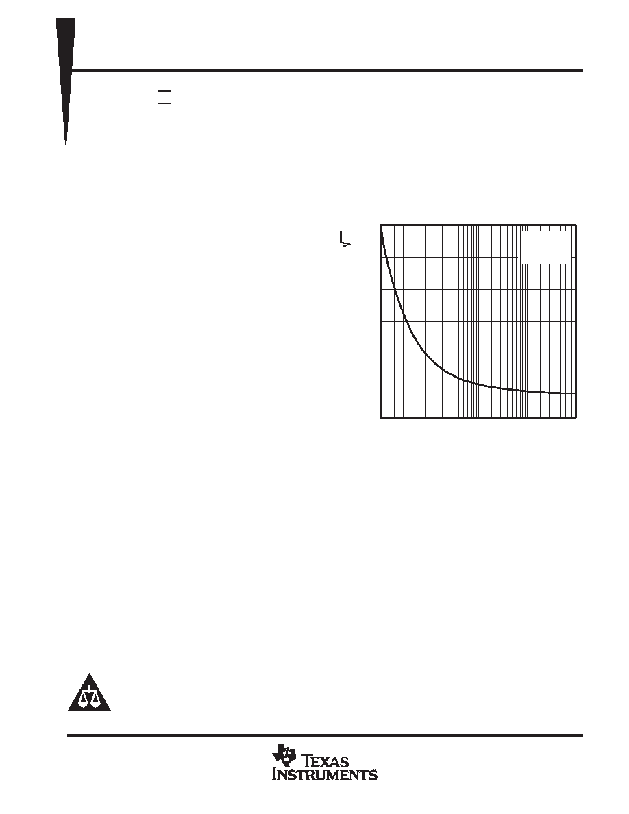
Vn
Equivalent
Input
Noise
V
oltage
nV/
Hz
f Frequency Hz
TYPICAL EQUIVALENT
INPUT NOISE VOLTAGE
vs
FREQUENCY
60
1 k
10 k
50
40
30
20
10
0
VDD = 5 V
RS = 20
TA = 25°C
Hz
V
n
Please be aware that an important notice concerning availability, standard warranty, and use in critical applications of
Texas Instruments semiconductor products and disclaimers thereto appears at the end of this data sheet.
相關(guān)PDF資料 |
PDF描述 |
|---|---|
| 5962-9088203QPA | OP-AMP, 400 uV OFFSET-MAX, 1.9 MHz BAND WIDTH, CDIP8 |
| 5962-9089401MEA | INSTRUMENTATION AMPLIFIER, 500 uV OFFSET-MAX, 4 MHz BAND WIDTH, CDIP16 |
| 5962-9089502MCA | OP-AMP, 50 uV OFFSET-MAX, 1.9 MHz BAND WIDTH, CDIP14 |
| 5962-9089502MPA | OP-AMP, 50 uV OFFSET-MAX, 1.9 MHz BAND WIDTH, CDIP8 |
| 5962-9089504QCA | OP-AMP, 40 uV OFFSET-MAX, 1.9 MHz BAND WIDTH, CDIP14 |
相關(guān)代理商/技術(shù)參數(shù) |
參數(shù)描述 |
|---|---|
| 5962-9088203V2A | 功能描述:運(yùn)算放大器 - 運(yùn)放 Low Noise Prec Adv LinCMOS Sgl Op Amp RoHS:否 制造商:STMicroelectronics 通道數(shù)量:4 共模抑制比(最小值):63 dB 輸入補(bǔ)償電壓:1 mV 輸入偏流(最大值):10 pA 工作電源電壓:2.7 V to 5.5 V 安裝風(fēng)格:SMD/SMT 封裝 / 箱體:QFN-16 轉(zhuǎn)換速度:0.89 V/us 關(guān)閉:No 輸出電流:55 mA 最大工作溫度:+ 125 C 封裝:Reel |
| 5962-9088204Q2A | 制造商:Texas Instruments 功能描述:OP Amp Dual GP R-R O/P ±8V/16V 20-Pin LCCC Tube |
| 5962-9088204QPA | 制造商:Texas Instruments 功能描述:OP Amp Dual GP R-R O/P 制造商:Rochester Electronics LLC 功能描述:- Bulk |
| 5962-9088801MRA | 制造商:Intersil Corporation 功能描述:SMD HD1-6409 CMOS MANCHESTER ENCODER-DECODER - Rail/Tube 制造商:Rochester Electronics LLC 功能描述:SMD HD1-6409 CMOS MANCHESTER ENCODER-DECODER - Bulk |
| 5962-9088901M2A | 制造商:Texas Instruments 功能描述:Buffer/Line Driver 4-CH Non-Inverting 3-ST BiCMOS 20-Pin LCCC Tube |
發(fā)布緊急采購,3分鐘左右您將得到回復(fù)。