- 您現(xiàn)在的位置:買(mǎi)賣(mài)IC網(wǎng) > PDF目錄56735 > 5962-9160201HZX 3-OUTPUT 15 W DC-DC REG PWR SUPPLY MODULE PDF資料下載
參數(shù)資料
| 型號(hào): | 5962-9160201HZX |
| 元件分類(lèi): | 電源模塊 |
| 英文描述: | 3-OUTPUT 15 W DC-DC REG PWR SUPPLY MODULE |
| 封裝: | FM-10 |
| 文件頁(yè)數(shù): | 4/7頁(yè) |
| 文件大?。?/td> | 55K |
| 代理商: | 5962-9160201HZX |
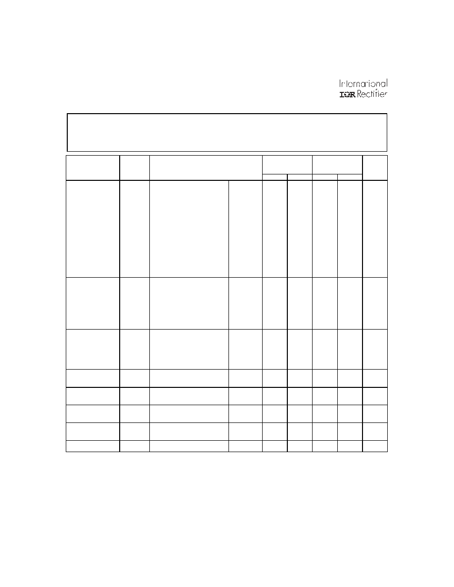
4
www.irf.com
ATO28XXT Series
T
CASE
= -55°C to +125°C, V
IN = +28V ± 5% unless otherwise specified
Specifications
ABSOLUTE MAXIMUM RATINGS
Input Voltage
-0.5V to 50V
Power Output
Internally limited, 17.5W typical
Soldering
300
°C for 10 seconds
Temperature Range
6
Operating
-55
°C to +135°C case
Storage
-65
°C to +135°C
Notes to Specifications
1.
Tested at each output.
2.
Parameter guaranteed by line and load regulation tests.
3.
At least 20 percent of the total output power should be taken from the (+5V volt) main output.
4.
Bandwidth guaranteed by design. Tested for 20KHz to 2MHz.
5.
An overload is that condition with a load in excess of the rated load but less than that necessary to trigger the short circuit
protection and is the condition of maximum power dissipation.
6.
Above 125
°C case temperature, derate output power linearly to 0 at 135°C case
TEST
SYMBOL
Condition
-55
°C ≤ T
C ≤
+125
°C, V
IN
= 28 V
DC ±
5%, C
L
=0
unless otherwise specified
ATO2812T/HB
ATO2815T/HB
Min
Max
Min
Max
Units
STATIC
CHARACTERISTICS
OUTPUT
Voltage
1
V
OUT
I
OUT = 0 (main)
I
OUT = 0 (dual)
1
TC = 25
°C
Over Temp
TC = 25
°C
Over Temp
4.95
4.90
±11.88
±11.76
5.05
5.10
±12.12
±12.24
4.95
4.90
±14.85
±14.70
5.05
5.10
±15.15
±15.30
V
Current
1,2,3
I
OUT
V
IN = 16, 28, and 40 VDC (main)
0.0
2000
0.0
2000
mA
Ripple Voltage
1,4
V
RIP
V
IN = 16, 28, and 40 VDC (dual)
1
V
IN = 16, 28, and 40 VDC
0.0
±208
80
0.0
±167
80
mA
mVp-p
BW = DC to 2 MHz (main)
V
IN = 16, 28, and 40 VDC
BW = DC to 2 MHz (dual))
40
mVp-p
Power
1,2,3
P
OUT
V
IN = 16, 28, and 40 VDC (main)
(+dual)
(-dual)
(total)
10
2.5
15
10
2.5
15
W
REGULATION
Line
1,3
Load
1,3
VR
LINE
VR
LOAD
V
IN = 16, 28, and 40 VDC
I
OUT = 0, 1000, 2000mA (main)
V
IN = 16, 28, and 40 VDC (dual)
I
OUT = 0, ±84, ±167mA (dual)
V
IN = 16, 28, and 40 VDC
I
OUT = 0, 1000, 2000mA (main)
V
IN = 16, 28, and 40 VDC
I
OUT = 0, ±84, ±167mA (dual)
TC = 25
°C
Over Temp
25
±30
±60
50
±60
25
±35
±75
50
±75
mV
INPUT
Current
Ripple Current
4
I
IN
I
RIP
I
OUT = 0, Inhibit (pin 8)
Tied to input return (pin 10)
I
OUT = 0, inhibit (pin 2) = open
I
OUT = 2000 mA (main)
I
OUT = ±167mA (dual)
BW = DC to 2MHz
15
40
50
15
40
50
mA
mAp-p
EFFICIENCY
E
FF
I
OUT = 2000mA (main)
I
OUT = ±167mA (dual)
TC =
±25°C
TC = 25
°C
76
%
ISOLATION
ISO
Input to output or any pin to
case (except pin 7) at 500 VDC,
TC = +25
°C
TC = 25
°C
100
M
Load Fault
Power Dissipation
3
P
D
Overload, TC = +25
°C5
Short Circuit, TC = +25
°C
TC = 25
°C
8
6
8
6
W
Switching Frequency
F
S
I
OUT = 2000mA (main)
I
OUT = ±167mA (dual)
225
275
225
275
KHz
Inhibit Open Circuit
Voltage
V
OI
9
13
9
13
V
相關(guān)PDF資料 |
PDF描述 |
|---|---|
| 5962-9161301HZX | 2-OUTPUT 30 W DC-DC REG PWR SUPPLY MODULE |
| 5962-9210901HZX | 2-OUTPUT 30 W DC-DC REG PWR SUPPLY MODULE |
| 5962-9210902HZX | 2-OUTPUT 30 W DC-DC REG PWR SUPPLY MODULE |
| 5962-9161302HZX | 2-OUTPUT 30 W DC-DC REG PWR SUPPLY MODULE |
| 5962-9161303HZX | 2-OUTPUT 30 W DC-DC REG PWR SUPPLY MODULE |
相關(guān)代理商/技術(shù)參數(shù) |
參數(shù)描述 |
|---|---|
| 5962-9160601M3A | 制造商:QP Semiconductor 功能描述:Flip Flop D-Type Bus Interface Pos-Edge 3-ST 1-Element 28-Pin CLLCC |
| 5962-9160601MLA | 制造商:QP Semiconductor 功能描述:Flip Flop D-Type Bus Interface Pos-Edge 3-ST 1-Element 24-Pin CDIP |
| 5962-9160901MLA | 制造商:QP Semiconductor 功能描述: |
| 5962-9161101MKA | 制造商:QP Semiconductor 功能描述:Flip Flop D-Type Bus Interface Pos-Edge 3-ST 1-Element 24-Pin CPAK |
| 5962-9161301HZA | 制造商:International Rectifier 功能描述:DC/DC CONVERTER, FLANGED, CLASS H - Rail/Tube |
發(fā)布緊急采購(gòu),3分鐘左右您將得到回復(fù)。