- 您現(xiàn)在的位置:買賣IC網(wǎng) > PDF目錄67335 > 5962-9169201QXC (MAXIM INTEGRATED PRODUCTS INC) 2-CH 16-BIT SUCCESSIVE APPROXIMATION ADC, SERIAL ACCESS, CDIP28 PDF資料下載
參數(shù)資料
| 型號(hào): | 5962-9169201QXC |
| 廠商: | MAXIM INTEGRATED PRODUCTS INC |
| 元件分類: | ADC |
| 英文描述: | 2-CH 16-BIT SUCCESSIVE APPROXIMATION ADC, SERIAL ACCESS, CDIP28 |
| 封裝: | CERAMIC, DIP-28 |
| 文件頁數(shù): | 12/39頁 |
| 文件大小: | 334K |
| 代理商: | 5962-9169201QXC |
第1頁第2頁第3頁第4頁第5頁第6頁第7頁第8頁第9頁第10頁第11頁當(dāng)前第12頁第13頁第14頁第15頁第16頁第17頁第18頁第19頁第20頁第21頁第22頁第23頁第24頁第25頁第26頁第27頁第28頁第29頁第30頁第31頁第32頁第33頁第34頁第35頁第36頁第37頁第38頁第39頁
MAX6954
4-Wire Interfaced, 2.7V to 5.5V LED Display
Driver with I/O Expander and Key Scan
2
_______________________________________________________________________________________
ABSOLUTE MAXIMUM RATINGS
Stresses beyond those listed under “Absolute Maximum Ratings” may cause permanent damage to the device. These are stress ratings only, and functional
operation of the device at these or any other conditions beyond those indicated in the operational sections of the specifications is not implied. Exposure to
absolute maximum rating conditions for extended periods may affect device reliability.
(Voltage with respect to GND.)
V+ .........................................................................-0.3V to +6V
All Other Pins............................................-0.3V to (V+ + 0.3V)
Current
O0–O7 Sink Current ......................................................935mA
O0–O18 Source Current .................................................55mA
DIN, CLK,
CS, OSC, DOUT, BLINK, OSC_OUT, ISET ....20mA
P0, P1, P2, P3, P4 ...........................................................40mA
GND .....................................................................................1A
Continuous Power Dissipation (TA = +70°C)
36-Pin SSOP (derate at 11.8mW/°C above +70°C) .....941mW
40-Pin PDIP (derate at 16.7mW/°C above +70°C).....1333mW
40-Pin TQFN (derate at 37mW/°C above +70°C) ......2963mW
Operating Temperature Range
(TMIN to TMAX) ...............................................-40°C to +125°C
Junction Temperature ......................................................+150°C
Storage Temperature Range .............................-65°C to +150°C
Lead Temperature (soldering, 10s) .................................+300°C
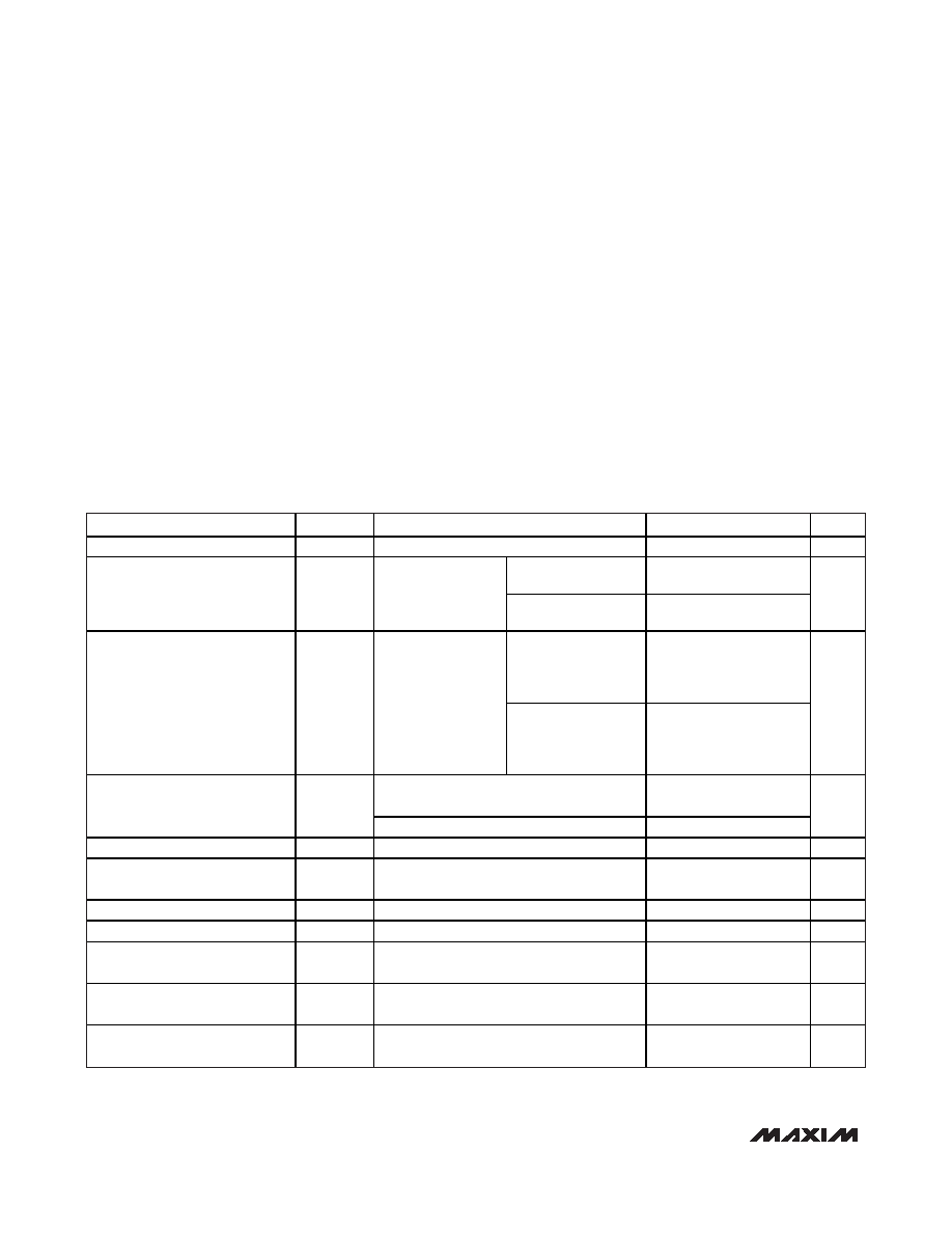
DC ELECTRICAL CHARACTERISTICS
(
Typical Operating Circuits, V+ = 2.7V to 5.5V, TA = TMIN to TMAX, unless otherwise noted.) (Note 1)
PARAMETER
SYMBOL
CONDITIONS
MIN
TYP
MAX
UNITS
Operating Supply Voltage
V+
2.7
5.5
V
TA = +25°C
10
35
Shutdown Supply Current
ISHDN
Shutdown mode, all
digital inputs at V+
or GND
TA = TMIN to TMAX
40
A
TA = +25°C
22
30
Operating Supply Current
I+
All segments on, all
digits scanned,
intensity set to full,
internal oscillator,
DOUT open circuit,
no display or
OSC_OUT load
connected
TA = TMIN to TMAX
35
mA
OSC = RC oscillator, RSET = 56k
Ω,
CSET = 22pF, V+ = 3.3V
4
Master Clock Frequency
fOSC
OSC driven externally
1
8
MHz
Dead Clock Protection Frequency
fOSC
95
kHz
OSC Internal/External Detection
Threshold
VOSC
1.7
V
OSC High Time
tCH
50
ns
OSC Low Time
tCL
50
ns
Slow Segment Blink Period
fSLOWBLINK
OSC = RC oscillator, RSET = 56k
Ω,
CSET = 22pF, V+ = 3.3V
1s
Fast Segment Blink Period
fFASTBLINK
OSC = RC oscillator, RSET = 56k
Ω,
CSET = 22pF, V+ = 3.3V
0.5
s
Fast or Slow Segment Blink Duty
Cycle
49.5
50.5
%
相關(guān)PDF資料 |
PDF描述 |
|---|---|
| 5962-9169301MCA | 4 CHANNEL, VIDEO AMPLIFIER, CDIP14 |
| 5962-9169401MCA | 1 CHANNEL, VIDEO AMPLIFIER, CDIP14 |
| 5962-9203101M2A | 1.5 A SWITCHING CONTROLLER, 1000 kHz SWITCHING FREQ-MAX, CQCC20 |
| 5962-9203101MEA | 1.5 A SWITCHING CONTROLLER, 1000 kHz SWITCHING FREQ-MAX, CDIP16 |
| 5962-9203103Q2A | 1.5 A SWITCHING CONTROLLER, 1000 kHz SWITCHING FREQ-MAX, CQCC20 |
相關(guān)代理商/技術(shù)參數(shù) |
參數(shù)描述 |
|---|---|
| 5962-9169301M2A | 制造商:Texas Instruments 功能描述:-LIFETIME BUYS TIL 03/03 |
| 5962-9169701MMA | 制造商:e2v Aerospace & Defense 功能描述:SMD MKD 87C51RC-16 PHI-JLCC |
| 5962-9169701MUA | 制造商:Rochester Electronics LLC 功能描述:- Bulk 制造商:Intel 功能描述: |
| 5962-9169702MUA | 制造商:Rochester Electronics LLC 功能描述:- Bulk |
| 5962-9172201MEA | 制造商:e2v 功能描述:Counter Single 4-Bit Binary UP 16-Pin CDIP 制造商:e2v technologies 功能描述:Counter Single 4-Bit Binary UP 16-Pin CDIP |
發(fā)布緊急采購,3分鐘左右您將得到回復(fù)。