- 您現(xiàn)在的位置:買賣IC網(wǎng) > PDF目錄56739 > 5962-9324601HXC (MS KENNEDY CORP) 1 CHANNEL, VIDEO AMPLIFIER, QFM24 PDF資料下載
參數(shù)資料
| 型號(hào): | 5962-9324601HXC |
| 廠商: | MS KENNEDY CORP |
| 元件分類: | 音頻/視頻放大 |
| 英文描述: | 1 CHANNEL, VIDEO AMPLIFIER, QFM24 |
| 封裝: | HERMETIC SEALED, QFP-24 |
| 文件頁數(shù): | 4/6頁 |
| 文件大小: | 220K |
| 代理商: | 5962-9324601HXC |
APPLICATION NOTES CON'T
Rev. A 5/02
4
OUTPUT CONNECTIONS
In applying the MSK 1901 in a system, two challenges
present themselves. The first challenge is to minimize
any stray capacitance from the output pin to ground.
Since the output connection is extremely susceptible to
capacitance loading, the elimination of ground planes
adjacent to the output and resistive load are important or
the rise and fall times will be limited. Keep output con-
nections as short as possible and insure that any ground
plane is at least one inch from the output signal.
The second challenge is to provide a very low
impedence connection between two sets of ground pins
(1, 2, 3, 4 and 15, 16, 17, 18). If mounting permits, the
best solution is to run a board ground track under the
MSK 1901 connecting the adjacent ground pins. How-
ever, the standard practice of heat sinking the MSK 1901
directly to the CRT chassis usually precludes this. A cut-
out is usually provided in the PC board where the MSK
1901 is surface mounted on the opposite side from the
other components. Two suggestions for this surface
mounting technique to improve performance are directed
at functionality or speed.
A functional solution is to run a ground trace on the
output pin side of the hybrid on the back side of the PC
board. The trace should be 0.1 to 0.2 inch necking down
to 0.1 inch as it perpendicularly crosses the output trace
on the other side of the board. This results in added
capacitance of only 0.1 to 0.4 pF.
A high speed solution is to have the ground cross the
input pin side of the hybrid. To counter the signal ground
disruption, the signal ground (pin 11) is internally con-
nected to the (15, 16, 17, 18) grounds. Use as broad a
ground trace as possible to improve stability.
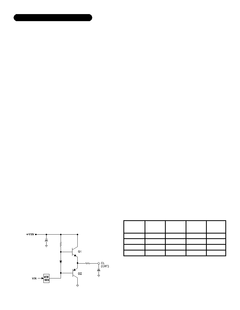
A third suggestion is to buffer the MSK 1901 using a
differential follower stage. This configuration as shown
in Figure 1 below allows an easier layout which mini-
mizes stray capacitance. The rise time is essentially lim-
ited by the capacitance of the output transistor and that
of Q1 and Q2.
Figure 1
POWER SUPPLIES
A +10V and a -10.5V power supply are required for
proper operation. These supplies can be set at ±12V for
convenience but this will increase the internal power dis-
sipation and package case temperature. VLRS can be any
voltage above VCB but not greater than VCB +65V. To
achieve maximum performance good high frequency
grounding practices and PC board layout are essential.
Proper power supply decoupling is also essential for
stability and good video performance. Place bypass ca-
pacitors as close to power supply pins as possible. Refer
to the typical connection circuit for recommended con-
nections.
POWER SUPPLY SEQUENCING
Power supply sequencing is necessary to avoid inter-
nal latch-up of the hybrid. External diodes should be placed
(anode to cathode) from VEE to GND, from GND to VCC
and from VCC to VLRS. If power supply sequencing is not
possible, all supplies should be applied to the hybrid within
5 mS of each other.
POWER DISSIPATION
The MSK 1901 power dissipation will vary depending
on load requirements and speed. The quad flat pack of
the hybrid is designed to provide a low thermal resis-
tance path from the hybrid circuit to an external heat
sink. Mounting flanges provide for excellent mechanical
and thermal attachment of the package to the heat sink.
In addition, the package is electrically isolated so that
mounting insulators are not needed and the heat sink
can be at any convenient potential. Refer to the follow-
ing table for typical power levels for selected video con-
ditions:
POWER DISSIPATION TABLE
(TC=25°C, VLRS=70V, RL=200)
VO -VBLACK
Duty
Cycle %
IC PD
Watts
PLOAD
Watts
TOTAL
PD Watts
0
100
80
0
35
50
1.6
7.8
6.5
5.6
0
6.1
4.9
10
1.6
13.9
11.4
15.6
When using multiple MSK 1901's, attach all devices
to a common heat sink (e.g. in a RGB system). This al-
lows close thermal tracking between hybrids and improves
color balance with varying input drive and ambient tem-
perature conditions. Common thermal tracking of the
devices reduces timing and other errors found in RGB
systems.
相關(guān)PDF資料 |
PDF描述 |
|---|---|
| 5962-9324601HXX | 1 CHANNEL, VIDEO AMPLIFIER, QFM24 |
| 5962-9325101MEA | ANALOG MULTIPLIER OR DIVIDER, 30 MHz BAND WIDTH, CDIP16 |
| 5962-9325101M2X | ANALOG MULTIPLIER OR DIVIDER, 30 MHz BAND WIDTH, CQCC20 |
| 5962-9325101MEX | ANALOG MULTIPLIER OR DIVIDER, 30 MHz BAND WIDTH, CDIP16 |
| 5962-9325101M2A | ANALOG MULTIPLIER OR DIVIDER, 30 MHz BAND WIDTH, CQCC20 |
相關(guān)代理商/技術(shù)參數(shù) |
參數(shù)描述 |
|---|---|
| 59629324903MXA | 制造商:IDT 功能描述:IDT7221L25LB |
| 5962-9324903MXA | 制造商:IDT 功能描述:IDT7221L25LB |
| 59629325101M2A | 制造商:HARRIS 功能描述:* |
| 5962-9325101M2A | 制造商:Rochester Electronics LLC 功能描述:- Bulk |
| 5962-9325301BCA | 制造商:QP Semiconductor 功能描述:BUFFER/LINE DRIVER 4-CH NON-INVERTING 3-ST CMOS 14-PIN CDIP 制造商:Texas Instruments 功能描述:Buffer/Line Driver 4-CH Non-Inverting 3-ST CMOS 14-Pin CDIP |
發(fā)布緊急采購,3分鐘左右您將得到回復(fù)。