- 您現(xiàn)在的位置:買賣IC網(wǎng) > PDF目錄67342 > 5962-9865901HXX (ANALOG DEVICES INC) DUAL 3-CH 12-BIT PROPRIETARY METHOD ADC, PARALLEL ACCESS, CQFP68 PDF資料下載
參數(shù)資料
| 型號(hào): | 5962-9865901HXX |
| 廠商: | ANALOG DEVICES INC |
| 元件分類: | ADC |
| 英文描述: | DUAL 3-CH 12-BIT PROPRIETARY METHOD ADC, PARALLEL ACCESS, CQFP68 |
| 封裝: | CERAMIC, LCC-68 |
| 文件頁(yè)數(shù): | 3/24頁(yè) |
| 文件大小: | 2403K |
| 代理商: | 5962-9865901HXX |
第1頁(yè)第2頁(yè)當(dāng)前第3頁(yè)第4頁(yè)第5頁(yè)第6頁(yè)第7頁(yè)第8頁(yè)第9頁(yè)第10頁(yè)第11頁(yè)第12頁(yè)第13頁(yè)第14頁(yè)第15頁(yè)第16頁(yè)第17頁(yè)第18頁(yè)第19頁(yè)第20頁(yè)第21頁(yè)第22頁(yè)第23頁(yè)第24頁(yè)
REV. A
AD10265
–11–
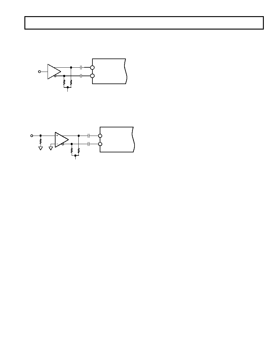
If a low jitter ECL clock is available, another option is to ac-couple
a differential ECL signal to the encode input pins as shown
below. The capacitors shown here should be chip capacitors,
but do not need to be of the low inductance variety.
ENCODE
AD10265
ECL
GATE
0.1 F
–VS
510
Figure 11. Differential ECL for Encode
As a final alternative, the ECL gate may be replaced by an ECL
comparator. The input to the comparator could then be a logic
signal or a sine signal.
ENCODE
AD10265
0.1 F
–VS
50
AD96687 (1/2)
510
Figure 12. ECL Comparator for Encode
USING THE FLEXIBLE INPUT
The AD10265 has been designed with the user’s ease of operation
in mind. Multiple input configurations have been included on
board to allow the user a choice of input signal levels and input
impedance. While the standard inputs are
±0.5 V, ±1.0 V, and
±2.0 V, the user can select the input impedance of the AD10265
on any input by using the other inputs as alternate locations for
GND or an external resistor. The following chart summarizes
the impedance options available at each input location:
AIN1 = 100
when AIN2 and AIN3 Are Open.
AIN1 = 75
when A
IN3 Is Shorted to GND.
AIN1 = 50
when AIN2 Is Shorted to GND.
AIN2 = 200
when AIN3 Is Open.
AIN2 = 100
when A
IN3 Is Shorted to GND.
AIN2 = 75
when AIN2 to AIN3 Has an External Resistor of
AIN2 = 300
, with AIN 3 Shorted to GND.
AIN2 = 50
when A
IN2 to AIN3 Has an External Resistor of
AIN2 = 100
, with AIN3 Shorted to GND.
AIN3 = 400
.
AIN3 = 100
when A
IN3 Has an External Resistor of 133
to GND.
AIN3 = 75
when AIN3 Has an External Resistor of 92 to GND.
AIN3 = 50
when AIN3 Has an External Resistor of 57 to GND.
GROUNDING AND DECOUPLING
Analog and Digital Grounding
Proper grounding is essential in any high speed, high resolution
system. Multilayer printed circuit boards (PCBs) are recom-
mended to provide optimal grounding and power schemes. The
use of ground and power planes offers distinct advantages:
1. The minimization of the loop area encompassed by a signal
and its return path.
2. The minimization of the impedance associated with ground
and power paths.
3. The inherent distributed capacitor formed by the power
plane, PCB insulation, and ground plane.
These characteristics result in both a reduction of electromagnetic
interference (EMI) and an overall improvement in performance.
It is important to design a layout that prevents noise from coupling
to the input signal. Digital signals should not be run in parallel
with input signal traces and should be routed away from the
input circuitry. The AD10265 does not distinguish between
analog and digital ground pins as the AD10265 should always
be treated as an analog component. All ground pins should be
connected together directly under the AD10265. The PCB
should have a ground plane covering all unused portions of the
component side of the board to provide a low impedance path
and manage the power and ground currents. The ground plane
should be removed from the area near the input pins to reduce
stray capacitance.
LAYOUT INFORMATION
The schematic of the evaluation board (Figure 13) represents
a typical implementation of the AD10265. The pinout of the
AD10265 is very straightforward and facilitates ease of use and
the implementation of high frequency/high resolution design
practices. It is recommended that high quality ceramic chip
capacitors be used to decouple each supply pin to ground directly
at the device. All capacitors can be standard high quality ceramic
chip capacitors.
Care should be taken when placing the digital output runs.
Because the digital outputs have such a high slew rate, the
capacitive loading on the digital outputs should be minimized.
Circuit traces for the digital outputs should be kept short and
connect directly to the receiving gate. Internal circuitry buffers
the outputs of the AD6640 ADC through a resistor network to
eliminate the need to externally isolate the device from the
receiving gate.
相關(guān)PDF資料 |
PDF描述 |
|---|---|
| 5962R0151901TXX | DUAL 3-CH 12-BIT PROPRIETARY METHOD ADC, PARALLEL ACCESS, CQFP68 |
| 5962-9954001NXD | 1-CH 10-BIT PROPRIETARY METHOD ADC, PARALLEL ACCESS, PDSO28 |
| TLC876CDB | 1-CH 10-BIT PROPRIETARY METHOD ADC, PARALLEL ACCESS, PDSO28 |
| TLC876CDW | 1-CH 10-BIT PROPRIETARY METHOD ADC, PARALLEL ACCESS, PDSO28 |
| TLC876IPW | 1-CH 10-BIT PROPRIETARY METHOD ADC, PARALLEL ACCESS, PDSO28 |
相關(guān)代理商/技術(shù)參數(shù) |
參數(shù)描述 |
|---|---|
| 5962-9866101QXA | 制造商:Texas Instruments 功能描述:5962-9866101QXA,C6X DSP,840 MFLOPS,CBGA - Rail/Tube 制造商:Texas Instruments 功能描述:SMV320C6701GLPW14 CLASS V DSP 840MFLOPS |
| 5962-9866101VXA | 功能描述:數(shù)字信號(hào)處理器和控制器 - DSP, DSC Rad-Tolerant Class V Fltg Pt Dig Sig Proc RoHS:否 制造商:Microchip Technology 核心:dsPIC 數(shù)據(jù)總線寬度:16 bit 程序存儲(chǔ)器大小:16 KB 數(shù)據(jù) RAM 大小:2 KB 最大時(shí)鐘頻率:40 MHz 可編程輸入/輸出端數(shù)量:35 定時(shí)器數(shù)量:3 設(shè)備每秒兆指令數(shù):50 MIPs 工作電源電壓:3.3 V 最大工作溫度:+ 85 C 封裝 / 箱體:TQFP-44 安裝風(fēng)格:SMD/SMT |
| 5962-9866102VXA | 制造商:Texas Instruments 功能描述:DIGITAL SIGNAL PROCESSOR |
| 59629873401CA | 制造商:Texas Instruments 功能描述:54ACTQ04DMBQ |
| 5962-98A1601VXA WAF | 制造商:Honeywell Sensing and Control 功能描述: |
發(fā)布緊急采購(gòu),3分鐘左右您將得到回復(fù)。