- 您現(xiàn)在的位置:買賣IC網(wǎng) > PDF目錄369226 > 66012-002 (MICROPAC INDUSTRIES INC) FOUR CHANNEL, HERMETICALLY SEALED, LOW-INPUT CURRENT, 6N140 OPTOCOUPLER PDF資料下載
參數(shù)資料
| 型號(hào): | 66012-002 |
| 廠商: | MICROPAC INDUSTRIES INC |
| 元件分類: | 光電耦合器 |
| 英文描述: | FOUR CHANNEL, HERMETICALLY SEALED, LOW-INPUT CURRENT, 6N140 OPTOCOUPLER |
| 中文描述: | 4 CHANNEL LOGIC OUTPUT OPTOCOUPLER |
| 封裝: | HERMETIC SEALED, DIP-16 |
| 文件頁(yè)數(shù): | 1/2頁(yè) |
| 文件大?。?/td> | 93K |
| 代理商: | 66012-002 |
MICROPAC INDUSTRIES, INC.
OPTOELECTRONIC PRODUCTS DIVISION
725 E. Walnut St., Garland, TX 75040
(972) 272-3571
Fax (972) 487-6918
www.micropac.com
E-MAIL: optosales@micropac.com
3 - 26
66012
FOUR CHANNEL, HERMETICALLY SEALED, LOW-INPUT
CURRENT, 6N140 OPTOCOUPLER
Mii
OPTOELECTRONIC PRODUCTS
DIVISION
Features:
DSCC Approved 8302401EX
High current transfer ratio: 1000% typical
1500 Vdc isolation test voltage
Low input current requirement: 0.5mA
Applications:
Military and Space
High reliability systems
Voltage Level Shifting
Isolated Receiver Input
Communication systems
DESCRIPTION
The
66012
optocoupler contains four infrared LEDs optically coupled to four corresponding high gain photon detectors. This
unique quad optocoupler provides high CTR and low leakage currents over the full military temperature range (-55
°
to
+125°C). The 66012 is a 16 pin dual-in-line, hermetically sealed package and is available in standard and MIL-PRF-38534
screened versions or tested to customer specifications.
ABSOLUTE MAXIMUM RATINGS
Storage Temperature........................................................................................................................................... -65°C to +150°C
Operating Free-Air Temperature Range............................................................................................................. -55°C to +125°C
Lead Solder Temperature.........................................................................................260°C for 10s (1.6mm below seating plane)
Peak Forward Input Current (each channel)............................................................................................... 20mA (1ms duration)
Average Forward Input Current ........................….(see Note 3).......................................................................................... 10mA
Reverse Input Voltage ...............................................................................................................................................................5V
Output Current - I
O
(each channel)...................................................................................................................................... 40mA
Output Power Dissipation (each channel) ..............(see Note 2)........................................................................................ 50mW
Supply Voltage - V
CC
............................................... (see Note 1) ............................................................................... -0.5 to 20V
Output Voltage - V
O
(each channel).……..............(see Note 1)............................................................................... . -0.5 to 20V
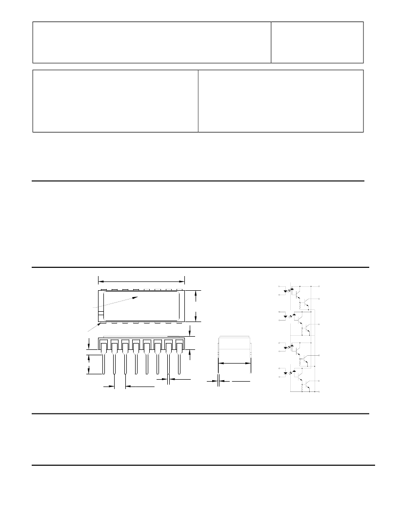
Package Dimensions Schematic Diagram
.290 [7.37]
.310 [7.87]
PIN 1
XXXX
Mii
6N140
.790 [20.06]
.820 [20.83]
0.170 [4.32
MAX]
0.150 [3.81]
.320 [8.13]
MAX
.020 [0.51]
ALL DIMENSIONS ARE IN INCHES [MILLIMETERS]
DATE CODE
8
K
7
A
A
5
K
6
GND
10
V04
11
V03
12
4
K
A
3
A
2
K
1
14V01
V02
13
VCC
15
0.20 [0.51]
MAX
.090 [2.29]
.110 [2.79]
.007 [0.18]
0.13 [0.33]
Notes:
1. Derate I
F
at 0.05 mA/°C above 25°C.
2. Collector output power plus one fourth of the total supply power is total output power. Derate at 0.46mW/°C above 25°C.
3. The lowest total I
OH
over temperature is developed by keeping V
CC
as low as possible, but greater that 2 volts. The
negative voltage at the detector side should be applied to Pin 10.
相關(guān)PDF資料 |
PDF描述 |
|---|---|
| 66012-003 | FOUR CHANNEL, HERMETICALLY SEALED, LOW-INPUT CURRENT, 6N140 OPTOCOUPLER |
| 66012-004 | FOUR CHANNEL, HERMETICALLY SEALED, LOW-INPUT CURRENT, 6N140 OPTOCOUPLER |
| 66013 | DUAL CHANNEL, HERMETICALLY SEALED, HIGH-SPEED 6N134 OPTOCOUPLER |
| 66013-000 | DUAL CHANNEL, HERMETICALLY SEALED, HIGH-SPEED 6N134 OPTOCOUPLER |
| 66013-001 | Circular Connector; MIL SPEC:MIL-C-26482, Series I; Body Material:Aluminum Alloy; Series:MS3122; Number of Contacts:55; Connector Shell Size:22; Connecting Termination:Crimp; Circular Shell Style:Box Mount Receptacle |
相關(guān)代理商/技術(shù)參數(shù) |
參數(shù)描述 |
|---|---|
| 66012-003 | 制造商:MII 制造商全稱:MII 功能描述:FOUR CHANNEL, HERMETICALLY SEALED, LOW-INPUT CURRENT, 6N140 OPTOCOUPLER |
| 66012-004 | 制造商:MII 制造商全稱:MII 功能描述:FOUR CHANNEL, HERMETICALLY SEALED, LOW-INPUT CURRENT, 6N140 OPTOCOUPLER |
| 6601-20-PPS | 制造商:SPC Multicomp 功能描述:IC SOCKET PLCC 20WAY TUBE/39 |
| 6601-20-PPS-18 | 制造商:SPC Multicomp 功能描述:IC SOCKET PLCC 20WAY |
| 6601-20-PPS-18-F6 | 制造商:SPC Multicomp 功能描述:SOCKET IC PLCC 20WAY 制造商:SPC Multicomp 功能描述:SOCKET IC, PLCC, 20WAY |
發(fā)布緊急采購(gòu),3分鐘左右您將得到回復(fù)。