- 您現(xiàn)在的位置:買(mǎi)賣(mài)IC網(wǎng) > PDF目錄360359 > 74ABT899 (NXP Semiconductors N.V.) 9-bit dual latch transceiver with 8-bit parity generator/checker 3-State PDF資料下載
參數(shù)資料
| 型號(hào): | 74ABT899 |
| 廠商: | NXP Semiconductors N.V. |
| 英文描述: | 9-bit dual latch transceiver with 8-bit parity generator/checker 3-State |
| 中文描述: | 9位雙鎖存器的8位奇偶發(fā)生器/檢查三態(tài) |
| 文件頁(yè)數(shù): | 5/16頁(yè) |
| 文件大小: | 123K |
| 代理商: | 74ABT899 |
第1頁(yè)第2頁(yè)第3頁(yè)第4頁(yè)當(dāng)前第5頁(yè)第6頁(yè)第7頁(yè)第8頁(yè)第9頁(yè)第10頁(yè)第11頁(yè)第12頁(yè)第13頁(yè)第14頁(yè)第15頁(yè)第16頁(yè)
Philips Semiconductors
Product specification
74ABT899
9-bit dual latch transceiver with 8-bit parity
generator/checker (3-State)
1998 Jan 16
5
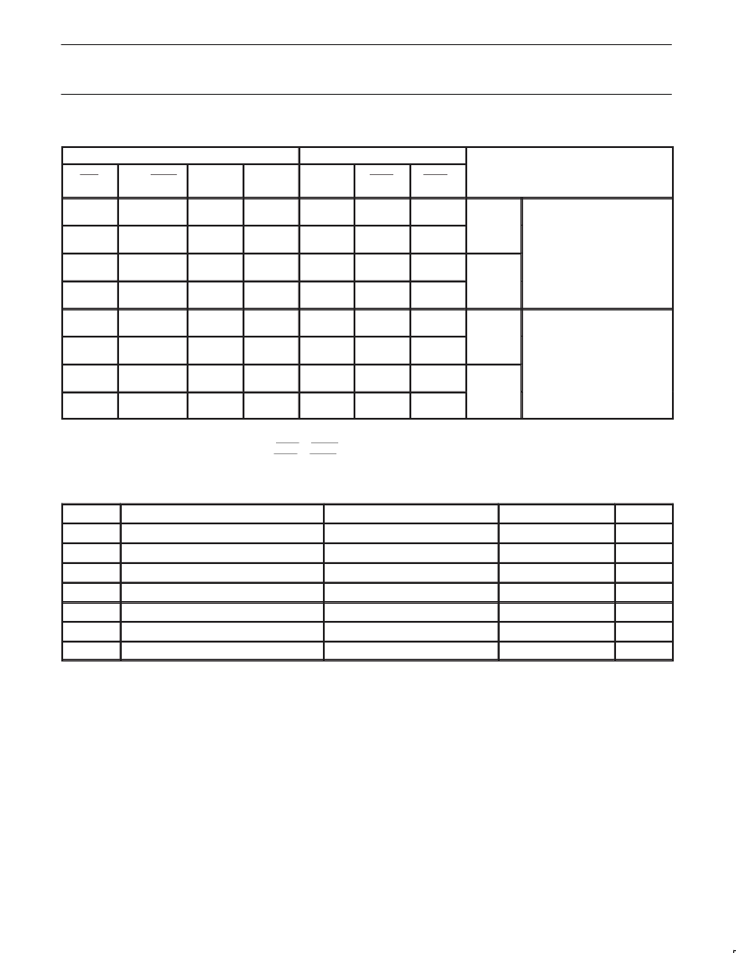
PARITY AND ERROR FUNCTION TABLE
INPUTS
OUTPUTS
SEL
ODD/EVEN
xPAR
(A or B)
Σ
of High
Inputs
xPAR
(B or A)
ERRt
ERRr*
PARITY MODES
H
H
H
Even
Odd
H
H
H
L
H
L
Odd
H
H
L
Even
Odd
L
L
L
H
L
H
Mode
Feed-through/check parity
H
L
H
Even
Odd
H
H
L
H
L
H
Even
H
L
L
Even
Odd
L
L
H
L
H
L
Mode
L
H
H
Even
Odd
H
L
H
L
H
H
Odd
L
H
L
Even
Odd
H
L
L
H
H
H
Mode
Generate parity
L
L
H
Even
Odd
L
H
L
H
H
H
Even
L
L
L
Even
Odd
L
H
H
L
H
H
Mode
H =
L
t
r
*
High voltage level
Low voltage level
Transmit–if the data path is from A
→
B then ERRt is ERRA
Receive–if the data path is from A
→
B then ERRr is ERRB
Blocked if latch is not transparent
=
=
=
ABSOLUTE MAXIMUM RATINGS
1, 2
SYMBOL
PARAMETER
CONDITIONS
RATING
UNIT
V
CC
DC supply voltage
–0.5 to +7.0
V
I
IK
DC input diode current
V
I
< 0
–18
mA
V
I
DC input voltage
3
–1.2 to +7.0
V
I
OK
DC output diode current
V
O
< 0
–50
mA
V
OUT
DC output voltage
3
output in Off or High state
–0.5 to +5.5
V
I
OUT
DC output current
output in Low state
128
mA
T
stg
Storage temperature range
–65 to 150
°
C
NOTES:
1. Stresses beyond those listed may cause permanent damage to the device. These are stress ratings only and functional operation of the
device at these or any other conditions beyond those indicated under “recommended operating conditions” is not implied. Exposure to
absolute-maximum-rated conditions for extended periods may affect device reliability.
2. The performance capability of a high-performance integrated circuit in conjunction with its thermal environment can create junction
temperatures which are detrimental to reliability. The maximum junction temperature of this integrated circuit should not exceed 1505C.
3. The input and output voltage ratings may be exceeded if the input and output current ratings are observed.
相關(guān)PDF資料 |
PDF描述 |
|---|---|
| 74ABT899 | Octal Buffers/Drivers With 3-State Outputs 20-SSOP 0 to 70 |
| 74ABT899CMSA | Octal Buffers/Drivers With 3-State Outputs 20-SSOP 0 to 70 |
| 74ABT899CSC | Octal Buffers/Drivers With 3-State Outputs 20-SOIC 0 to 70 |
| 74ABT899CMSAX | Industry-Standard, 12-Bit ADC with Reference |
| 74ABT899CQCX | Single 8-bit Bus Transceiver |
相關(guān)代理商/技術(shù)參數(shù) |
參數(shù)描述 |
|---|---|
| 74ABT899_ZAF3026B WAF | 制造商:Fairchild Semiconductor Corporation 功能描述: |
| 74ABT899A | 功能描述:總線(xiàn)收發(fā)器 9-BIT LATCH XCVR W/PARITY 3-S RoHS:否 制造商:Fairchild Semiconductor 邏輯類(lèi)型:CMOS 邏輯系列:74VCX 每芯片的通道數(shù)量:16 輸入電平:CMOS 輸出電平:CMOS 輸出類(lèi)型:3-State 高電平輸出電流:- 24 mA 低電平輸出電流:24 mA 傳播延遲時(shí)間:6.2 ns 電源電壓-最大:2.7 V, 3.6 V 電源電壓-最小:1.65 V, 2.3 V 最大工作溫度:+ 85 C 封裝 / 箱體:TSSOP-48 封裝:Reel |
| 74ABT899A,602 | 功能描述:總線(xiàn)收發(fā)器 9-BIT LATCH XCVR RoHS:否 制造商:Fairchild Semiconductor 邏輯類(lèi)型:CMOS 邏輯系列:74VCX 每芯片的通道數(shù)量:16 輸入電平:CMOS 輸出電平:CMOS 輸出類(lèi)型:3-State 高電平輸出電流:- 24 mA 低電平輸出電流:24 mA 傳播延遲時(shí)間:6.2 ns 電源電壓-最大:2.7 V, 3.6 V 電源電壓-最小:1.65 V, 2.3 V 最大工作溫度:+ 85 C 封裝 / 箱體:TSSOP-48 封裝:Reel |
| 74ABT899A,623 | 功能描述:總線(xiàn)收發(fā)器 9-BIT LATCH XCVR RoHS:否 制造商:Fairchild Semiconductor 邏輯類(lèi)型:CMOS 邏輯系列:74VCX 每芯片的通道數(shù)量:16 輸入電平:CMOS 輸出電平:CMOS 輸出類(lèi)型:3-State 高電平輸出電流:- 24 mA 低電平輸出電流:24 mA 傳播延遲時(shí)間:6.2 ns 電源電壓-最大:2.7 V, 3.6 V 電源電壓-最小:1.65 V, 2.3 V 最大工作溫度:+ 85 C 封裝 / 箱體:TSSOP-48 封裝:Reel |
| 74ABT899A-T | 功能描述:總線(xiàn)收發(fā)器 9-BIT LATCH XCVR W/PARITY 3-S RoHS:否 制造商:Fairchild Semiconductor 邏輯類(lèi)型:CMOS 邏輯系列:74VCX 每芯片的通道數(shù)量:16 輸入電平:CMOS 輸出電平:CMOS 輸出類(lèi)型:3-State 高電平輸出電流:- 24 mA 低電平輸出電流:24 mA 傳播延遲時(shí)間:6.2 ns 電源電壓-最大:2.7 V, 3.6 V 電源電壓-最小:1.65 V, 2.3 V 最大工作溫度:+ 85 C 封裝 / 箱體:TSSOP-48 封裝:Reel |
發(fā)布緊急采購(gòu),3分鐘左右您將得到回復(fù)。