- 您現(xiàn)在的位置:買賣IC網(wǎng) > PDF目錄360419 > 74B2529 PDF資料下載
參數(shù)資料
| 型號(hào): | 74B2529 |
| 文件頁數(shù): | 1/8頁 |
| 文件大小: | 132K |
| 代理商: | 74B2529 |
TL/F/11923
C
September 1995
CGS64/74B2529
500 ps 2 to 10 Minimum Skew Clock Driver
General Description
This minimum skew clock driver is designed for Clock Gen-
eration and Support (CGS) applications operating from
33 MHz to 80 MHz. The devices guarantee minimum output
skew across the outputs of a given device.
Skew parameters are also provided as a means to measure
duty cycle requirements as those found in high speed clock-
ing systems. The ’2529 is a minimum skew clock driver with
two selectable inputs driving ten outputs.
The SEL pin is used to determine which CLKn will have an
active effect on the outputs of the circuit. When SEL
e
1,
the CLK1 input is selected and when SEL
e
0, the CLK0
input is selected. The non-selected CLKn input will not have
any effect on the logical output level of the circuit. The out-
put pins act as a single entity and will follow the state of the
CLK inputs.
Features
Y
Clock Generation and Support (CGS) devices
Y
Ideal for high frequency signal generation or clock
distribution applications
Y
CGS74B version features National’s Advanced Bipolar
FAST
é
LSI process
Y
2-to-10 low skew clock distribution
Y
500 ps pin-to-pin output skew (V package)
Y
Specification for transition skew to meet duty cycle
requirements
Y
20-center pin V
CC
and GND configuration or PLCC to
minimize high speed switching noise
Y
Current sourcing 48 mA and current sinking of 64 mA
Y
Low dynamic power consumption above 20 MHz
Y
Guaranteed 4 kV ESD protection
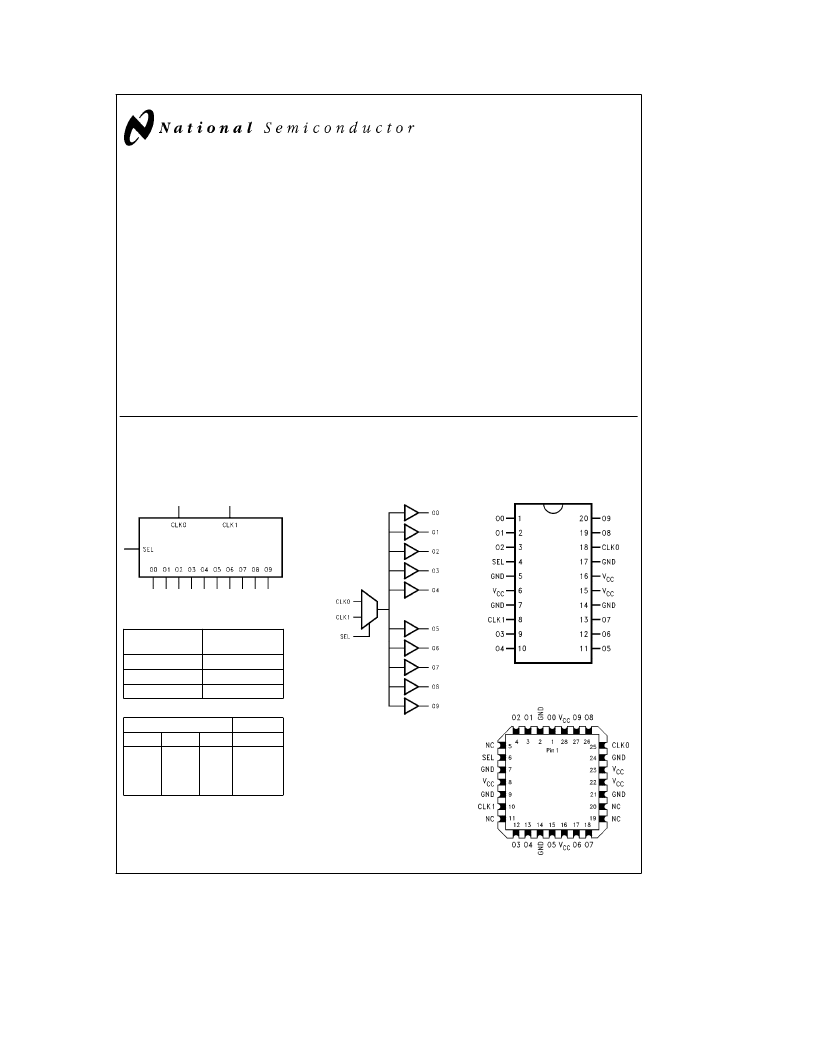
Logic Symbols
TL/F/11923–1
Pin Descriptlon
Pin
Description
Names
CLK0, CLK1
Clock Input
O0–O9
Outputs
SEL
Clock Select
Inputs
Outputs
CLK0
CLK1
SEL
O0–O9
L
H
X
X
X
X
L
H
L
L
H
H
L
H
L
H
L
e
Low Logic Level
H
e
High Logic Level
X
e
Immaterial
TL/F/11923–2
Connection Diagrams
Pin Assignment
SOIC
TL/F/11923–3
Pin Assignment
for PLCC
TL/F/11923–4
FAST
é
is a registered trademark of National Semiconductor Corporation.
C
1996 National Semiconductor Corporation
RRD-B30M106/Printed in U. S. A.
http://www.national.com
相關(guān)PDF資料 |
PDF描述 |
|---|---|
| 74B304 | |
| 74B305 | |
| 74BCT2828ASCQR | 10-Bit Buffer/Driver |
| 74BCT2952SCQR | Single 8-bit Bus Transceiver |
| 74BCT374PCQR | Octal D-Type Flip-Flop |
相關(guān)代理商/技術(shù)參數(shù) |
參數(shù)描述 |
|---|---|
| 74B-3 | 制造商:Cooper Bussmann 功能描述:AT&T COLUMBUS FUSE - Bulk 制造商:COOPER BUSSMANN 功能描述:AT&T COLUMBUS FUSE |
| 74BB | 功能描述:沖壓機(jī)與沖模 PUN.UNIT(COND) 1-1/4 RoHS:否 制造商:Souriau 大小: 產(chǎn)品:Dies 類型:Crimping 描述/功能: |
| 74BC645AFP-E | 制造商:Renesas Electronics 功能描述:Cut Tape 制造商:Renesas 功能描述:Bus XCVR Single 8-CH 3-ST 20-Pin SOP Tube |
| 74BCT125SC | 制造商:Rochester Electronics LLC 功能描述:- Bulk |
| 74BCT2240PC | 制造商:Rochester Electronics LLC 功能描述:- Bulk |
發(fā)布緊急采購,3分鐘左右您將得到回復(fù)。