- 您現(xiàn)在的位置:買賣IC網(wǎng) > PDF目錄360419 > 74B304 PDF資料下載
參數(shù)資料
| 型號(hào): | 74B304 |
| 文件頁數(shù): | 3/6頁 |
| 文件大小: | 122K |
| 代理商: | 74B304 |
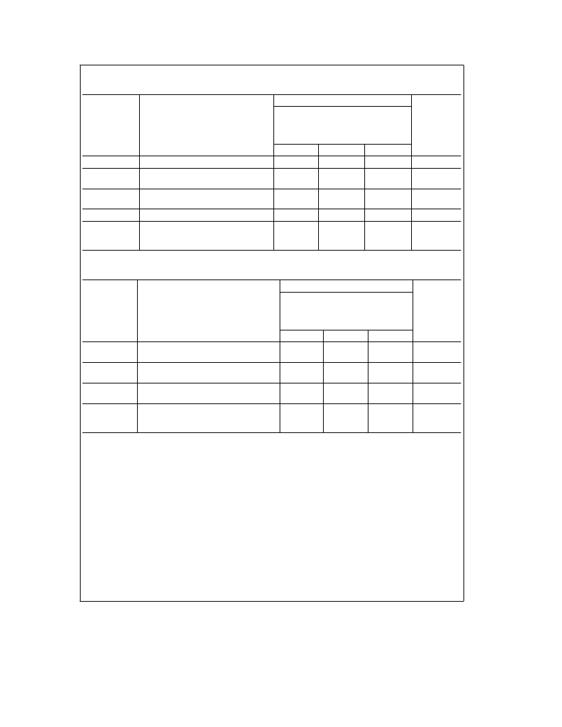
AC Electrical Characteristics
Over recommended operating conditions unless specified otherwise. All typical values are measured at V
CC
e
5V, T
A
e
25
§
C
Symbol
Parameter
CGS74B304
Units
V
CC
e
4.5V to 5.5V
T
A
e
0
§
C to
a
70
§
C
C
L
e
0 pF–50 pF
R
L
e
500
X
Min
Typ
Max
f
MAX
Maximum Input Frequency (Note 2)
110
MHz
t
PLH
,
t
PHL
Propagation Delay CLKn to O
n
(Note 2)
4
8.5
ns
t
PLH
,
t
PHL
Propagation Delay PRE/CLR
(Note 2)
4
11
ns
t
SU
Set Up Time before CLK
5
ns
t
W
CLK HI
CLK LO
CLR/PRE
4
4
4
ns
Extended AC Electrical Characteristics
Over recommended operating conditions unless specified otherwise. All typical values are measured at V
CC
e
5V, T
A
e
25
§
C
Symbol
Parameter
CGS74B304
Units
V
CC
e
4.5V to 5.5V
T
A
e
0
§
C to
a
70
§
C
C
L
e
0 pF–50 pF
R
L
e
500
X
Min
Typ
Max
t
OSHL Q
Maximum Skew Common Edge
Output-to-Output Variation (Notes 1, 2)
0.5
ns
t
OSLH Q
Maximum Skew Common Edge
Output-to-Output Variation (Notes 1, 2)
0.5
ns
t
PS
Maximum Skew. Pin (Signal)
Transition Variation (Note 1)
1.1
ns
t
rise
,
t
fall
Rise/Fall Time
(from 0.8V/2.0V to 2.0V/0.8V)
0 pF–30 pF Loads (Note 2)
1.1
0.9
2.0
2.0
ns
Note 1:
Output-to-Output Skew is defined as the absolute value of the difference between the actual propagation delay for any outputs within the same packaged
device. The specifications apply to any outputs switching in the same direction either HIGH to LOW (t
OSHL
) or LOW to HIGH (t
OSLH
) or in opposite directions both
HL and LH (t
OST
). Parameters t
OST
and t
PS
guaranteed by design.
Note 2:
This device is sensitive to noise due to the large transient currents which occur during multiple switching of the outputs. V
CC
bypass capacitor(s), chip
types, must be placed as closely as possible to the V
CC
pin.
Note 3:
Refer to Minimum Skew Parameters Measurement Information Chart for definitions of each skew specification.
Note 4:
All input pulses are from 3.5V to 0.3V with rise and fall times of 2.0 ns.
Note 5:
Load capacitance includes the test jig.
http://www.national.com
3
相關(guān)PDF資料 |
PDF描述 |
|---|---|
| 74B305 | |
| 74BCT2828ASCQR | 10-Bit Buffer/Driver |
| 74BCT2952SCQR | Single 8-bit Bus Transceiver |
| 74BCT374PCQR | Octal D-Type Flip-Flop |
| 74BCT374SCQR | Octal D-Type Flip-Flop |
相關(guān)代理商/技術(shù)參數(shù) |
參數(shù)描述 |
|---|---|
| 74BB | 功能描述:沖壓機(jī)與沖模 PUN.UNIT(COND) 1-1/4 RoHS:否 制造商:Souriau 大小: 產(chǎn)品:Dies 類型:Crimping 描述/功能: |
| 74BC645AFP-E | 制造商:Renesas Electronics 功能描述:Cut Tape 制造商:Renesas 功能描述:Bus XCVR Single 8-CH 3-ST 20-Pin SOP Tube |
| 74BCT125SC | 制造商:Rochester Electronics LLC 功能描述:- Bulk |
| 74BCT2240PC | 制造商:Rochester Electronics LLC 功能描述:- Bulk |
| 74BCT2241SC | 制造商:Rochester Electronics LLC 功能描述:- Bulk 制造商:Texas Instruments 功能描述: |
發(fā)布緊急采購,3分鐘左右您將得到回復(fù)。