- 您現(xiàn)在的位置:買賣IC網(wǎng) > PDF目錄360427 > 74F164N (NXP SEMICONDUCTORS) 8-bit serial-in parallel-out shift register PDF資料下載
參數(shù)資料
| 型號: | 74F164N |
| 廠商: | NXP SEMICONDUCTORS |
| 元件分類: | 通用總線功能 |
| 英文描述: | 8-bit serial-in parallel-out shift register |
| 中文描述: | F/FAST SERIES, 8-BIT RIGHT SERIAL IN PARALLEL OUT SHIFT REGISTER, TRUE OUTPUT, PDIP14 |
| 封裝: | PLASTIC, DIP-14 |
| 文件頁數(shù): | 4/10頁 |
| 文件大?。?/td> | 83K |
| 代理商: | 74F164N |
Philips Semiconductors
Product specification
74F164
8-bit serial-in parallel-out shift register
1995 Sep 22
4
DC ELECTRICAL CHARACTERISTICS
(Over recommended operating free-air temperature range unless otherwise noted.)
SYMBOL
PARAMETER
TEST
LIMITS
UNIT
CONDITIONS
1
MIN
TYP
2
MAX
V
OH
High-level output voltage
High-level out ut voltage
V
= MIN, V
= MAX,
CC
V
IH
= MIN, I
OH
= MAX
±
10%V
CC
±
5%V
CC
±
10%V
CC
±
5%V
CC
2.5
V
IL
2.7
3.4
V
V
OL
Low-level output voltage
V
= MIN, V
= MAX,
CC
V
IH
= MIN, I
OL
= MAX
0.30
0.50
V
IL
0.30
0.50
V
V
IK
I
I
I
IH
I
ILL
I
OS
I
CC
Input clamp voltage
V
CC
= MIN, I
I
= I
IK
V
CC
= MAX, V
I
= 7.0V
V
CC
= MAX, V
I
= 2.7V
V
CC
= MAX, V
I
= 0.5V
V
CC
= MAX
V
CC
= MAX
–0.73
–1.2
V
Input current at maximum input voltage
100
μ
A
μ
A
High-level input current
20
Low-level input current
–0.6
mA
Short-circuit output current
3
-60
–150
mA
Supply current (total)4
33
55
mA
Notes to DC electrical characteristics
1. For conditions shown as MIN or MAX, use the appropriate value specified under recommended operating conditions for the applicable type.
2. All typical values are at V
CC
= 5V, T
amb
= 25
°
C.
3. Not more than one output should be shorted at a time. For testing I
OS
, the use of high-speed test apparatus and/or sample-and-hold
techniques are preferable in order to minimize internal heating and more accurately reflect operational values. Otherwise, prolonged shorting
of a High output may raise the chip temperature well above normal and thereby cause invalid readings in other parameter tests. In any
sequence of parameter test, I
OS
tests should be performed last.
4. Measure I
CC
with the serial inputs grounded, the clock input at 2.4V, and a momentary ground, then applied to Master Reset, and all outputs
open.
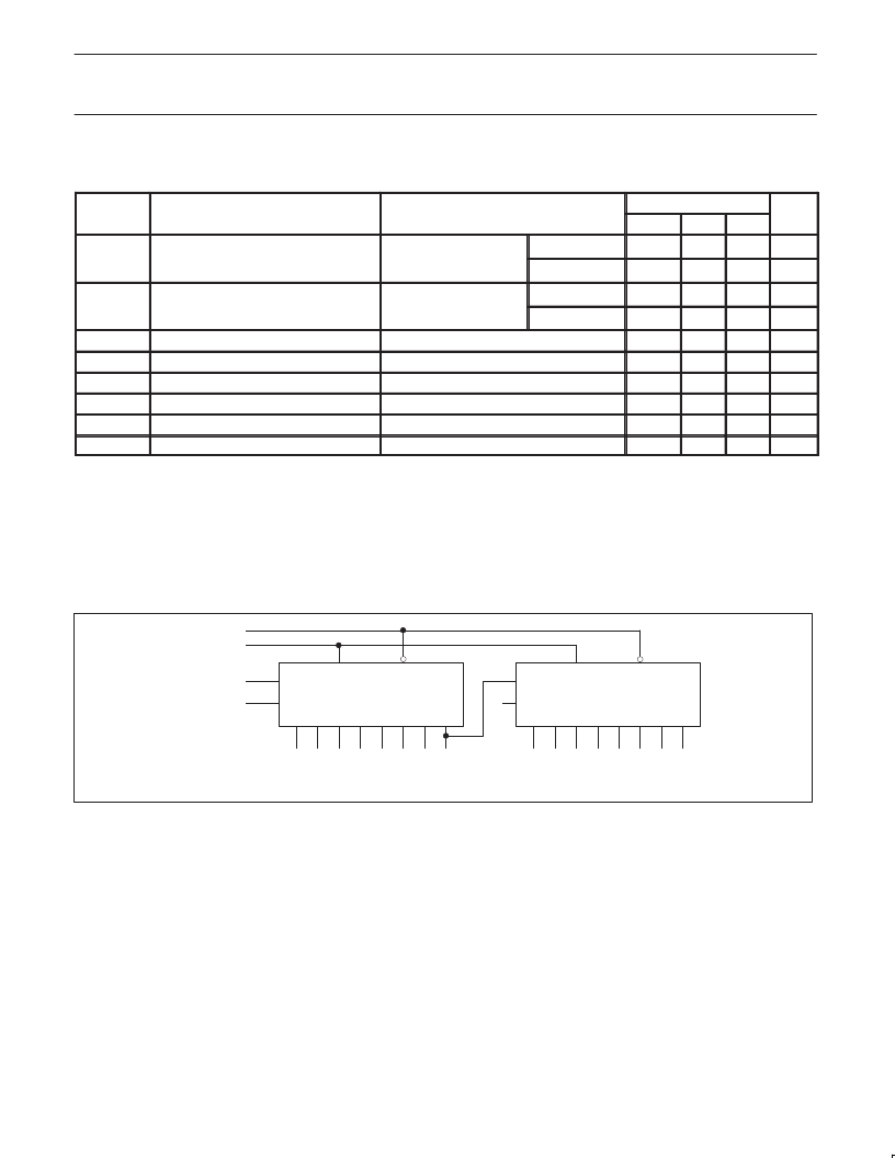
APPLICATION
RESET
CLOCK
DATA
ENABLE
Dsa
Dsb
Dsa
Dsb
CP
MR
D0
D1
D2
D3
D4
D5
D6
D7
D8
D9
D10 D11 D12 D13 D14 D15
CP
MR
H
74F164
74F164
Q0
Q1
Q2
Q3
Q4
Q5
Q6
Q7
Q0
Q1
Q2
Q3
Q4
Q5
Q6
Q7
SF00716
The 74F164 can be cascaded to form synchronous shift registers of longer length.
Here, two devices are combined to form a 16-bit shift register.
相關(guān)PDF資料 |
PDF描述 |
|---|---|
| 74F164AFM | Serial-In, Parallel-Out Shift Register |
| 74F164ALM | Serial-In, Parallel-Out Shift Register |
| 74F164APC | Serial-In, Parallel-Out Shift Register |
| 74F164ASC | Serial-In, Parallel-Out Shift Register |
| 74F164ASJ | Serial-In, Parallel-Out Shift Register |
相關(guān)代理商/技術(shù)參數(shù) |
參數(shù)描述 |
|---|---|
| 74F164PC | 制造商:Rochester Electronics LLC 功能描述:- Bulk |
| 74F166 | 制造商:PHILIPS 制造商全稱:NXP Semiconductors 功能描述:8-bit bidirectional universal shift register |
| 74F166D | 制造商:NXP Semiconductors 功能描述: |
| 74F166N | 制造商:NXP Semiconductors 功能描述: |
| 74F168DC | 制造商:FAIR 功能描述:Counter, Up/Down, Decade, 16 Pin, Ceramic, DIP |
發(fā)布緊急采購,3分鐘左右您將得到回復(fù)。