- 您現(xiàn)在的位置:買賣IC網(wǎng) > PDF目錄360546 > 7ABT2240PWDH (NXP SEMICONDUCTORS) Octal inverting buffer with 30ohm series termination resistors 3-State PDF資料下載
參數(shù)資料
| 型號: | 7ABT2240PWDH |
| 廠商: | NXP SEMICONDUCTORS |
| 元件分類: | 通用總線功能 |
| 英文描述: | Octal inverting buffer with 30ohm series termination resistors 3-State |
| 中文描述: | ABT SERIES, DUAL 4-BIT DRIVER, INVERTED OUTPUT, PDSO20 |
| 封裝: | 4.40 MM, PLASTIC, TSSOP-20 |
| 文件頁數(shù): | 4/10頁 |
| 文件大小: | 103K |
| 代理商: | 7ABT2240PWDH |
Philips Semiconductors
Octal inverting buffer with 30
series termination
resistors (3-State)
Product specification
74ABT2240
1998 Jan 16
4
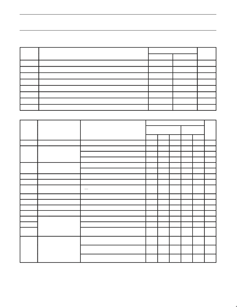
RECOMMENDED OPERATING CONDITIONS
SYMBOL
PARAMETER
LIMITS
UNIT
Min
Max
V
CC
DC supply voltage
4.5
5.5
V
V
I
Input voltage
0
V
CC
V
V
IH
High-level input voltage
2.0
V
V
IL
Low-level Input voltage
0.8
V
I
OH
High-level output current
–32
mA
I
OL
Low-level output current
12
mA
t/
v
Input transition rise or fall rate
0
10
ns/V
T
amb
Operating free-air temperature range
–40
+85
°
C
DC ELECTRICAL CHARACTERISTICS
LIMITS
SYMBOL
PARAMETER
TEST CONDITIONS
T
amb
= +25
°
C
T
amb
= –40
°
C
to +85
°
C
UNIT
Min
Typ
Max
Min
Max
V
IK
Input clamp voltage
V
CC
= 4.5V; I
IK
= –18mA
V
CC
= 4.5V; I
OH
= –3mA; V
I
= V
IL
or V
IH
V
CC
= 5.0V; I
OH
= –3mA; V
I
= V
IL
or V
IH
V
CC
= 4.5V; I
OH
= –32mA; V
I
= V
IL
or V
IH
V
CC
= 4.5V; I
OL
= 5mA; V
I
= V
IL
or V
IH
;
V
CC
= 4.5V; I
OL
= 12mA; V
I
= V
IL
or V
IH
V
CC
= 5.5V; V
I
= GND or 5.5V
V
CC
= 0.0V; V
O
or V
I
≤
4.5V
V
CC
= 2.1V; V
= 0.5V; V
I
= GND or V
CC
;
V
OE
= Don’t care
V
CC
= 5.5V; V
O
= 2.7V; V
I
= V
IL
or V
IH
V
CC
= 5.5V; V
O
= 0.5V; V
I
= V
IL
or V
IH
V
CC
= 5.5V; V
O
= 5.5V; V
I
= GND or V
CC
V
CC
= 5.5V; V
O
= 2.5V
V
CC
= 5.5V; Outputs High, V
I
= GND or V
CC
V
CC
= 5.5V; Outputs Low, V
I
= GND or V
CC
V
CC
= 5.5V; Outputs 3-State;
V
I
= GND or V
CC
Outputs enabled, one data input at 3.4V,
other inputs at V
CC
or GND; V
CC
= 5.5V
Outputs 3-State, one data input at 3.4V,
other inputs at V
CC
or GND; V
CC
= 5.5V
Outputs 3-State, one enable input at 3.4V,
other inputs at V
CC
or GND; V
CC
= 5.5V
–0.9
–1.2
–1.2
V
2.5
2.9
2.5
V
V
OH
High-level output voltage
3.0
3.4
3.0
V
2.0
2.4
2.0
V
V
OL
Low-level output voltage
0.32
0.55
0.55
V
0.8
0.8
V
I
I
Input leakage current
±
0.01
±
1.0
±
1.0
μ
A
I
OFF
Power-off leakage current
±
5.0
±
100
±
100
μ
A
I
PU/PD
Power–up/down 3-State
output current
3
±
5.0
±
50
±
50
μ
A
I
OZH
I
OZL
I
CEX
I
O
I
CCH
I
CCL
3-State output High current
0.01
50
50
μ
A
μ
A
3-State output Low current
–0.01
–50
–50
Output high leakage current
5.0
50
50
μ
A
Output current
1
–50
–100
–180
–50
–180
mA
50
250
250
μ
A
Quiescent supply current
24
30
30
mA
I
CCZ
50
250
250
μ
A
0.5
1.5
1.5
mA
I
CC
Additional supply current per
input pin
2
50
250
250
μ
A
0.5
1.5
1.5
mA
NOTES:
1. Not more than one output should be tested at a time, and the duration of the test should not exceed one second.
2. This is the increase in supply current for each input at 3.4V.
3. This parameter is valid for any V
CC
between 0V and 2.1V, with a transition time of up to 10msec. From V
CC
= 2.1V to V
CC
= 5V
±
10% a
transition time of up to 100
μ
sec is permitted.
相關(guān)PDF資料 |
PDF描述 |
|---|---|
| 7ABT2241PWDH | Power Supply |
| 7ABT2244PWDH | Octal buffer/line driver with 30ohm series termination resistors 3-State |
| 7ABT2245PWDH | Octal transceiver with direction pin with 30ohm series termination resistors 3-State |
| 7ABT273APWDH | Octal D-type flip-flop |
| 7ABT2952PWDH | Octal registered transceiver 3-State |
相關(guān)代理商/技術(shù)參數(shù) |
參數(shù)描述 |
|---|---|
| 7ABT2241PWDH | 制造商:PHILIPS 制造商全稱:NXP Semiconductors 功能描述:Octal buffer with 30ohm series termination resistors; 3-State |
| 7ABT2244PWDH | 制造商:PHILIPS 制造商全稱:NXP Semiconductors 功能描述:Octal buffer/line driver with 30ohm series termination resistors 3-State |
| 7ABT2245PWDH | 制造商:PHILIPS 制造商全稱:NXP Semiconductors 功能描述:Octal transceiver with direction pin with 30ohm series termination resistors 3-State |
| 7ABT273APWDH | 制造商:PHILIPS 制造商全稱:NXP Semiconductors 功能描述:Octal D-type flip-flop |
| 7ABT2952PWDH | 制造商:PHILIPS 制造商全稱:NXP Semiconductors 功能描述:Octal registered transceiver 3-State |
發(fā)布緊急采購,3分鐘左右您將得到回復(fù)。