- 您現(xiàn)在的位置:買賣IC網(wǎng) > PDF目錄369357 > 7B991 (Maxwell Technologies, Inc) Programmable Skew Clock Buffer (PSCB) PDF資料下載
參數(shù)資料
| 型號(hào): | 7B991 |
| 廠商: | Maxwell Technologies, Inc |
| 英文描述: | Programmable Skew Clock Buffer (PSCB) |
| 中文描述: | 可編程偏移時(shí)鐘緩沖器(PSCB) |
| 文件頁(yè)數(shù): | 4/17頁(yè) |
| 文件大?。?/td> | 253K |
| 代理商: | 7B991 |
第1頁(yè)第2頁(yè)第3頁(yè)當(dāng)前第4頁(yè)第5頁(yè)第6頁(yè)第7頁(yè)第8頁(yè)第9頁(yè)第10頁(yè)第11頁(yè)第12頁(yè)第13頁(yè)第14頁(yè)第15頁(yè)第16頁(yè)第17頁(yè)

M
4
All data sheets are subject to change without notice
2002 Maxwell Technologies.
All rights reserved.
Programmable Skew Clock Buffer (PSCB)
7B991
09.23.02 Rev 4
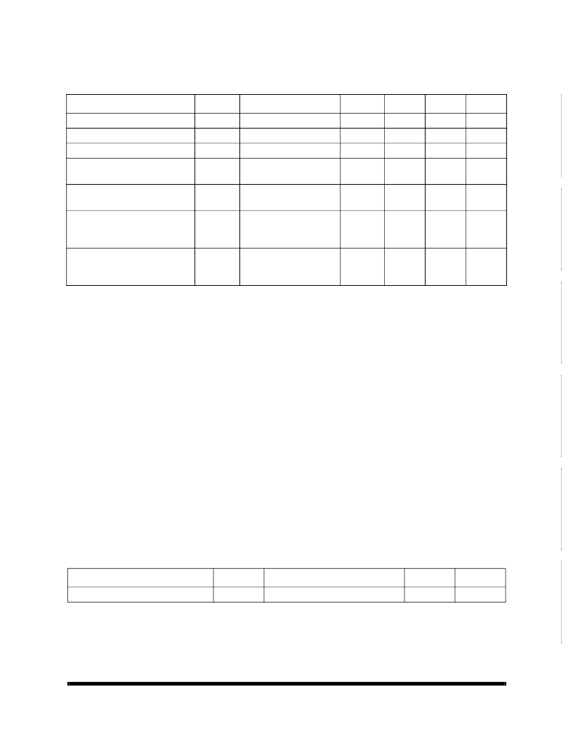
Input HIGH Current (Test, FS, xFn)
Input MID Current (Test, FS, xFn)
Input LOW Current (Test, FS, xFn)
Output Short Circuit (Test, FS, xFn)
2
I
IH
I
IMM
I
ILL
I
OS
V
IN
= V
CC
V
IN
= 2.75
V
IN
= GND
V
CC
= Max., V
OUT
= GND
(25
°
C only)
V
CCN
= V
CCQ
= Max, all input
selects open
V
CCN
= V
CCQ
= Max,
I
OUT
= 0 mA,
Input selects open, fMAX
V
CCN
= V
CCQ
= Max,
I
OUT
= 0 mA
Input selects open, fMAX
1, 2, 3
1, 2, 3
1, 2, 3
1
--
200
200
-200
-250
μA
μA
μA
mA
-200
--
--
Operating Current used by Internal
Circuitry
Output Buffer Current per Output
Pair
3
I
CCQ
1, 2, 3
--
90
mA
I
CCN
1, 2, 3
--
14
mA
Power Dissipation per Output Pair
4
P
D
1, 2, 3
--
78
mW
1. These inputs are normally wired to V
CC
,GND, or left unconnected (actual threshold voltages vary as a percentage of V
CC
). Inter-
nal termnation resistors hold unconnected inputs at V
CC
/2. If these inputs are switched, the function and timng of the outputs
may glitch and the PLL may require an additional t
LOCK
time before all datasheet limts are achieved.
2. This device should be tested one output at a time, output shorted for less than one second, less than 10% duty cycle. Room
temperature only.
3. Total output current per output pair can be approximated by the following expression that includes device current plus load cur-
rent:
ICCN = [(4 + 0.11F) + [((835-3F)/Z) + (.0022FC)]N] x 1.1
Where:
f = frequency in MHz
C = capacitive load in pF
Z = line impedance in ohms
N = number of loaded outputs; 0, 1, or 2
FC = F *C
4. Total power dissipation per output pair can be approximated by the following expression that includes device power dissipation
due to the load circuit:
PD = [(22 + 0.61F) + [((1550-2.7F)/Z) + (.0125FC)]N] x 1.1
T
ABLE
6. 7B991 C
APACITANCE1
1. Guaranteed by design.
P
ARAMETER
S
YMBOL
T
EST
C
ONDITIONS
M
AX
U
NIT
Input Capacitance
C
IN
T
A
= 25
°
C, f = 1 MHz, V
CC
= 5.0V
10
pF
T
ABLE
5. 7B991 DC E
LECTRICAL
C
HARACTERISTICS
(V
CC
= 5V ±10%, T
A
= -40
TO
85
°
C,
UNLESS
OTHERWISE
SPECIFIED
)
S
YMBOL
T
EST
C
ONDITIONS
P
ARAMETER
S
UBGROUPS
M
IN
M
AX
U
NIT
相關(guān)PDF資料 |
PDF描述 |
|---|---|
| 7BT2F9A-361 | HIGH CAPACITY ENVIRONMENTALLY SEALED |
| 7BT2 | HIGH CAPACITY ENVIRONMENTALLY SEALED |
| 7BT2F15A-361 | HIGH CAPACITY ENVIRONMENTALLY SEALED |
| 7BT2F15A-362 | HIGH CAPACITY ENVIRONMENTALLY SEALED |
| 7BT2L9F-364 | HIGH CAPACITY ENVIRONMENTALLY SEALED |
相關(guān)代理商/技術(shù)參數(shù) |
參數(shù)描述 |
|---|---|
| 7B9910-5SI | 制造商: 功能描述: 制造商:undefined 功能描述: |
| 7B9910A-5SZI | 制造商:Cypress Semiconductor 功能描述: |
| 7B9910A-7SI | 制造商:Cypress Semiconductor 功能描述: |
| 7B9910A-SZC | 制造商:Cypress Semiconductor 功能描述: |
| 7B9910AT | 制造商:Cypress Semiconductor 功能描述: |
發(fā)布緊急采購(gòu),3分鐘左右您將得到回復(fù)。