- 您現(xiàn)在的位置:買賣IC網(wǎng) > PDF目錄252165 > 805J500471MCTE03 (SYFER TECHNOLOGY LTD) 1 FUNCTIONS, 50 V, FEED THROUGH CAPACITOR PDF資料下載
參數(shù)資料
| 型號: | 805J500471MCTE03 |
| 廠商: | SYFER TECHNOLOGY LTD |
| 元件分類: | 數(shù)據(jù)傳輸濾波器 |
| 英文描述: | 1 FUNCTIONS, 50 V, FEED THROUGH CAPACITOR |
| 封裝: | EIA STD PACKAGE SIZE 0603, CERAMIC PACKAGE-3 |
| 文件頁數(shù): | 3/4頁 |
| 文件大小: | 194K |
| 代理商: | 805J500471MCTE03 |

Integrated Passive Components
Balanced Line EMI Chip
BLC
The Syfer Balanced Line EMI chip has a unique internal architecture
which provides unbeatable EMC performance for dual line data
transmission.
C1
LINE A
LINE B
C1
C2
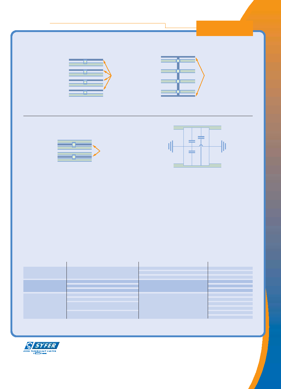
The Balanced Line EMI chip replaces decoupling capacitors or 3
terminal feedthrough chips on a 1 for 2 basis and provides line to
line (differential mode) decoupling. Fig 2.
The internal structure furnishes a reduced inductance when
compared to that of a conventional capacitor. This is a result of the
novel internal electrode structure which inherently reduces the
inductance by the cancellation effect of opposing currents in close
proximity.
The capacitance line to ground (common mode) is closely matched
due to the symmetry within the design. As the device includes line
to ground capacitance for both lines, any temperature, ageing and
voltage effects will have an equal influence on both lines therefore
maintaining balanced decoupling.
The construction also allows a capacitance between lines as well as
to ground as shown in Fig 3.
INPUT 2
INPUT 1
INPUT 3
INPUT 4
CHIP CAPACITORS
EARTH
TRACKS
INPUT 2
INPUT 1
INPUT 3
INPUT 4
3 TERMINAL CHIPS
EARTH
TRACKS
BALANCED LINE
EMI CHIP
EARTH
TRACKS
INPUT 2
INPUT 1
INPUT 3
INPUT 4
Fig 1
Fig 2
Fig 3
C2, the line to line capacitance, is half the line to ground
capacitance thus providing coupling of high frequency interference
between balanced lines.
Because the part acts as a decoupling device, the current limitations
of a standard 3 terminal chip do not apply. The single line 3
terminal feedthrough chip carries the signal current through the
very thin feedthrough electrodes within the device which have
limited DC resistance and so can cause excessive heating, hence the
maximum permissible current is often limited to around 300 mA for
a 1206 device. The dual line 3 terminal chip is in by-pass across
two lines and so is unaffected by high signal currents.
Table 1 offers a comparison of decoupling devices and
demonstrates how the Balanced Line EMI chip extends the options
for EMC circuit protection.
Component
Advantages
Disadvantages
Applications
● Requires 1 per line
● By-pass
Chip capacitor
● Industry standard
● High inductance
● Low frequency
● Capacitance matching problems
3 terminal
● Feedthrough
feedthrough
● Lower Inductance
● Current limited
● Unbalanced lines
● High frequency
● Very low inductance
● By-pass
● Replaces 2 (or 3) components
● Balanced lines
Balanced line
● Negates the effects of
● Not for unbalanced signal lines
● High frequency
EMI chip
temperature, voltage and ageing
● DC electric motors
● Provides both common mode and
differential mode attenuation
Table 1
A typical application for dual line data transmission would see a
board layout using decoupling chip capacitors or 3 terminal
feedthrough chips as shown in Fig 1.
61
相關PDF資料 |
PDF描述 |
|---|---|
| 805J500473MXBE03 | 1 FUNCTIONS, 50 V, FEED THROUGH CAPACITOR |
| 805J500473MXRE03 | 1 FUNCTIONS, 50 V, FEED THROUGH CAPACITOR |
| 805J500473MXTE03 | 1 FUNCTIONS, 50 V, FEED THROUGH CAPACITOR |
| 88H1.8 | 1 FUNCTIONS, 8.83 MHz, 0.45 kHz BW(delta f), DISCRETE CRYSTAL FILTER |
| 80L14C | FAST BLOW ELECTRIC FUSE, 80A, 600VAC, 250VDC, 200000A (IR), INLINE/HOLDER |
相關代理商/技術參數(shù) |
參數(shù)描述 |
|---|---|
| 805JR005E | 制造商:OHMITE 制造商全稱:Ohmite Mfg. Co. 功能描述:Metal-Mite? Aluminum Housed Axial Term. Wirewound, 1% Tolerance |
| 805JR10E | 制造商:OHMITE 制造商全稱:Ohmite Mfg. Co. 功能描述:Metal-Mite? Aluminum Housed Axial Term. Wirewound, 1% Tolerance |
| 805L | 制造商:SIPEX 制造商全稱:Sipex Corporation 功能描述:Low Power Microprocessor Supervisory with Battery Switch-Over |
| 805M | 制造商:SIPEX 制造商全稱:Sipex Corporation 功能描述:Low Power Microprocessor Supervisory with Battery Switch-Over |
| 805M1-0020 | 功能描述:加速計 - 板上安裝 AC Resp Accel WB Hi-Res 20g FS RoHS:否 制造商:Murata 傳感軸:Double 加速:12 g 靈敏度: 封裝 / 箱體: 輸出類型:Analog 數(shù)字輸出 - 位數(shù):11 bit 電源電壓-最大:5.25 V 電源電壓-最小:4.75 V 電源電流:4 mA 最大工作溫度:+ 125 C 最小工作溫度:- 40 C |
發(fā)布緊急采購,3分鐘左右您將得到回復。