- 您現(xiàn)在的位置:買賣IC網(wǎng) > PDF目錄378210 > 80960CF-33 (Intel Corp.) 32-Bit High-Performance Superscalar Embedded Microprocessor(32位高性能超標(biāo)量嵌入式微處理器) PDF資料下載
參數(shù)資料
| 型號(hào): | 80960CF-33 |
| 廠商: | Intel Corp. |
| 英文描述: | 32-Bit High-Performance Superscalar Embedded Microprocessor(32位高性能超標(biāo)量嵌入式微處理器) |
| 中文描述: | 32位高性能嵌入式微處理器超標(biāo)量(32位高性能超標(biāo)量嵌入式微處理器) |
| 文件頁(yè)數(shù): | 30/77頁(yè) |
| 文件大小: | 927K |
| 代理商: | 80960CF-33 |
第1頁(yè)第2頁(yè)第3頁(yè)第4頁(yè)第5頁(yè)第6頁(yè)第7頁(yè)第8頁(yè)第9頁(yè)第10頁(yè)第11頁(yè)第12頁(yè)第13頁(yè)第14頁(yè)第15頁(yè)第16頁(yè)第17頁(yè)第18頁(yè)第19頁(yè)第20頁(yè)第21頁(yè)第22頁(yè)第23頁(yè)第24頁(yè)第25頁(yè)第26頁(yè)第27頁(yè)第28頁(yè)第29頁(yè)當(dāng)前第30頁(yè)第31頁(yè)第32頁(yè)第33頁(yè)第34頁(yè)第35頁(yè)第36頁(yè)第37頁(yè)第38頁(yè)第39頁(yè)第40頁(yè)第41頁(yè)第42頁(yè)第43頁(yè)第44頁(yè)第45頁(yè)第46頁(yè)第47頁(yè)第48頁(yè)第49頁(yè)第50頁(yè)第51頁(yè)第52頁(yè)第53頁(yè)第54頁(yè)第55頁(yè)第56頁(yè)第57頁(yè)第58頁(yè)第59頁(yè)第60頁(yè)第61頁(yè)第62頁(yè)第63頁(yè)第64頁(yè)第65頁(yè)第66頁(yè)第67頁(yè)第68頁(yè)第69頁(yè)第70頁(yè)第71頁(yè)第72頁(yè)第73頁(yè)第74頁(yè)第75頁(yè)第76頁(yè)第77頁(yè)
80960CF-40, -33, -25, -16
A
24
PRELIMINARY
4.3
Recommended Connections
Power and ground connections must be made to
multiple V
and V
(GND) pins. Every 80960CF-
based circuit board should include power (V
) and
ground (V
) planes for power distribution. Every
V
pin must be connected to the power plane, and
every V
pin must be connected to the ground
plane. Pins identified as “NC”
must not
be
connected in the system.
Liberal decoupling capacitance should be placed
near the 80960CF. The processor can cause tran-
sient power surges when its numerous output buffers
transition, particularly when connected to large
capacitive loads.
Low inductance capacitors and interconnects are
recommended for best high frequency electrical
performance. Inductance can be reduced by short-
ening the board traces between the processor and
decoupling capacitors as much as possible. Capaci-
tors specifically designed for PGA packages will offer
the lowest possible inductance.
For reliable operation, always connect unused inputs
to an appropriate signal level. In particular, any
unused interrupt (XINT, NMI), DMA (DREQ), or
BTERM input should be connected to V
through a
pull-up resistor. Pull-up resistors should be in the in
the range of 20 K
for each pin tied high. If READY
or HOLD are not used, the unused input should be
connected to ground.
N.C. pins must always
remain unconnected.
For additional information
refer to the i960
Cx Microprocessor User’s Manual
(270710).
4.4
DC Specifications
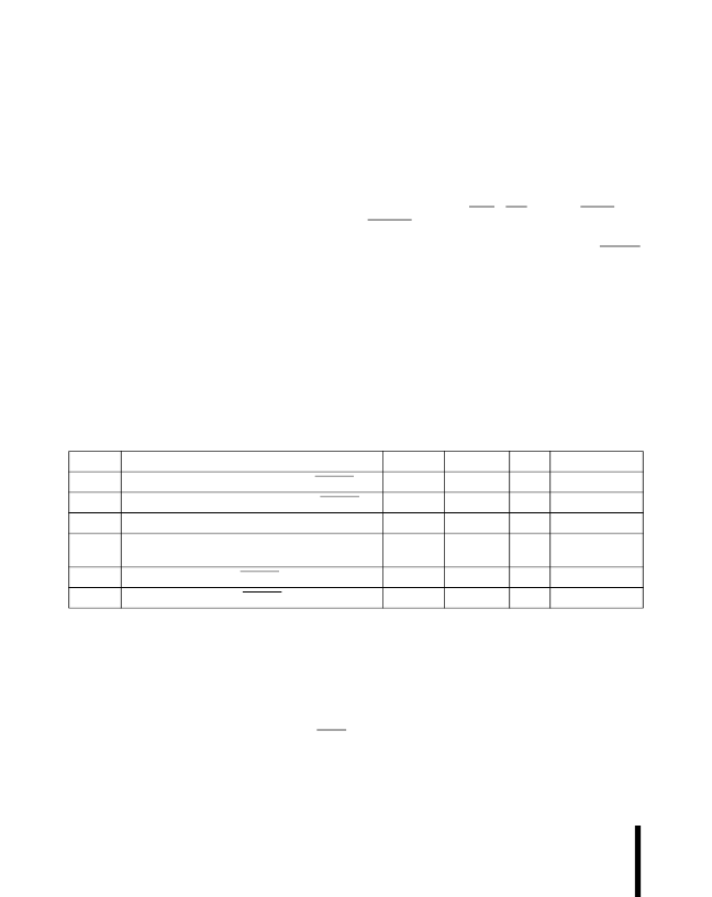
Table 14. DC Characteristics
(Sheet 1 of 2)
(80960CF-40, 33, -25, -16 under the conditions described in
Section 4.2, Operating Conditions
.)
Symbol
Parameter
Min
Max
Units
Notes
V
IL
V
IH
V
OL
V
OH
Input
Low
Voltage for all pins except RESET
– 0.3
+0.8
V
Input High Voltage for all pins except RESET
2.0
V
CC
+ 0.3
0.45
V
Output Low Voltage
V
I
OL
= 5 mA
Output High Voltage
I
OH
= –1 mA
I
OH
= – 200
μ
A
2.4
V
CC
– 0.5
– 0.3
V
V
V
ILR
V
IHR
NOTES:
1. No pullup or pulldown.
2. These pins have internal pullup resistors.
3. These pins have internal pulldown resistors.
4. Measured at worst case frequency, V
and temperature, with device operating and outputs loaded to the test conditions
described in
Section 4.5.1, AC TEST CONDITIONS.
5. I
CC
Typical is not tested.
6. Output Capacitance is the capacitive load of a floating output.
7. CLKMODE pin has a pulldown resistor only when ONCE pin is deasserted.
Input Low Voltage for RESET
1.5
V
Input High Voltage for RESET
3.5
V
CC
+ 0.3
V
相關(guān)PDF資料 |
PDF描述 |
|---|---|
| 80960CF-40 | 32-Bit High-Performance Superscalar Embedded Microprocessor(32位高性能超標(biāo)量嵌入式微處理器) |
| 80960CF | 32-Bit High-Performance Superscalar Processor(32位高性能超標(biāo)量處理器) |
| 80960JD | EMBEDDED 32-BIT MICROPROCESSOR |
| 80960JT | EMBEDDED 32-BIT MICROPROCESSOR |
| 80960JF | 3.3 V EMBEDDED 32-BIT MICROPROCESSOR |
相關(guān)代理商/技術(shù)參數(shù) |
參數(shù)描述 |
|---|---|
| 80960CF-40 | 制造商:INTEL 制造商全稱:Intel Corporation 功能描述:80960CF-40, -33, -25, -16 32-BIT HIGH-PERFORMANCE SUPERSCALAR EMBEDDED MICROPROCESSOR |
| 80960HA | 制造商:INTEL 制造商全稱:Intel Corporation 功能描述:80960HA/HD/HT 32-Bit High-Performance Superscalar Processor |
| 80960HD | 制造商:INTEL 制造商全稱:Intel Corporation 功能描述:80960HA/HD/HT 32-Bit High-Performance Superscalar Processor |
| 80960HT | 制造商:INTEL 制造商全稱:Intel Corporation 功能描述:80960HA/HD/HT 32-Bit High-Performance Superscalar Processor |
| 80960JA | 制造商:INTEL 制造商全稱:Intel Corporation 功能描述:EMBEDDED 32-BIT MICROPROCESSOR |
發(fā)布緊急采購(gòu),3分鐘左右您將得到回復(fù)。