- 您現(xiàn)在的位置:買賣IC網(wǎng) > PDF目錄371713 > 8P4SMA (NEC Corp.) 8A MOLD ISOLATED SCR PDF資料下載
參數(shù)資料
| 型號(hào): | 8P4SMA |
| 廠商: | NEC Corp. |
| 英文描述: | 8A MOLD ISOLATED SCR |
| 中文描述: | 8A條模具隔震可控硅 |
| 文件頁數(shù): | 2/6頁 |
| 文件大小: | 238K |
| 代理商: | 8P4SMA |
Data Sheet D17164EJ3V0DS
2
8P2SMA,8P4SMA
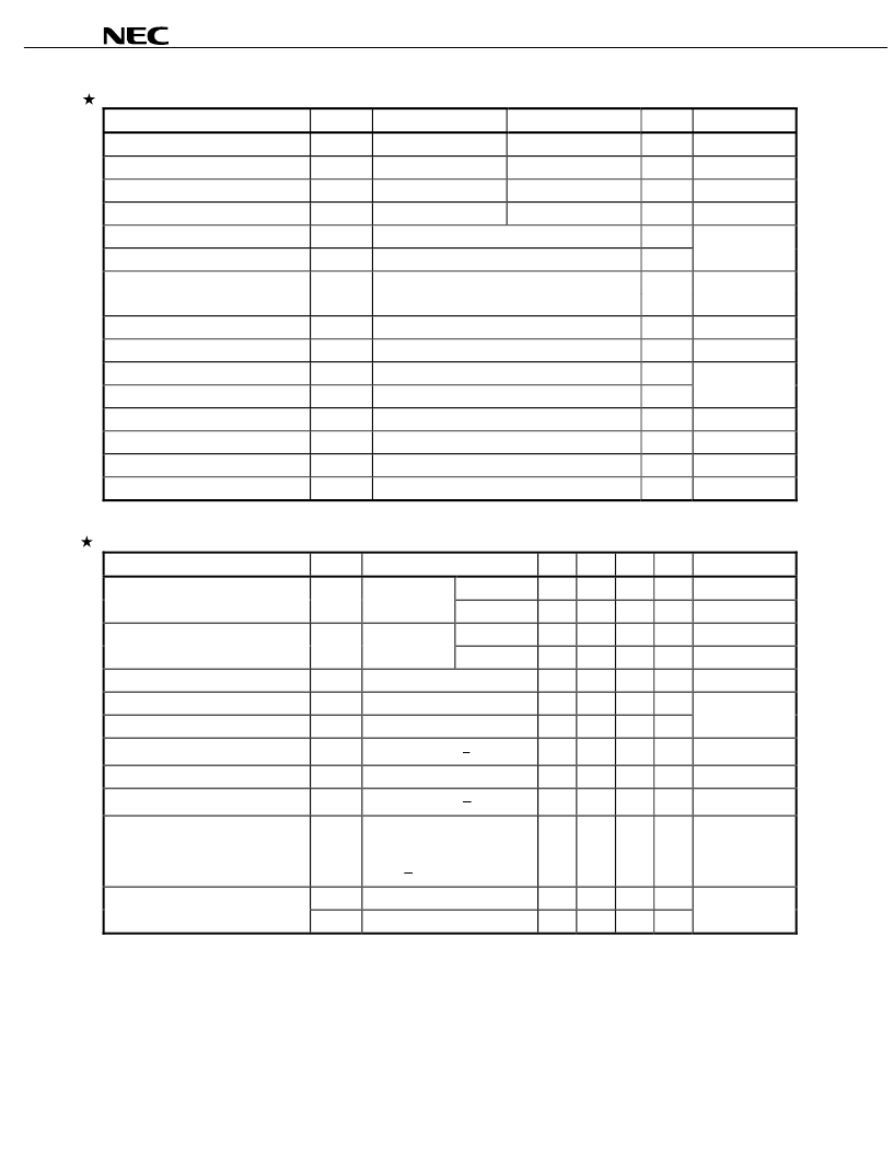
MAXIMUM RATINGS
Parameter
Symbol
8P2SMA
8P4SMA
Unit
Remarks
Non-repetitive Peak Reverse Voltage
V
RSM
300
500
V
Non-repetitive Peak Off-state Voltage
V
DSM
300
500
V
Repetitive Peak Reverse Voltage
V
RRM
200
400
V
Repetitive Peak Off-state Voltage
V
DRM
200
400
V
Average On-state Current
I
T(AV)
8 (T
C
= 88°C, single phase half wave,
θ
= 180°)
A
Refer to
Figure 11
Effective On-state Current
I
T(RMS)
12.6
A
and
12
.
Surge On-state Current
I
TSM
100 (f = 50 Hz, sine half wave, 1 cycle)
A
Refer to
Figure 2
.
110 (f = 60 Hz, sine half wave, 1 cycle)
Fusing Current
∫
i
T2
dt
45 (1 ms
≤
t
≤
10 ms)
A
2
s
Critical Rate Rise of On-state Current
dI
T
/dt
50
A/
μ
s
Peak Gate Power Dissipation
P
GM
5 (f
≥
50 Hz, Duty
≤
10%)
W
Refer to
Figure 3
.
Average Gate Power Dissipation
P
G(AV)
0.5
W
Peak Gate Forward Current
I
FGM
2 (f
≥
50 Hz, Duty
≤
10%)
A
Peak Gate Reverse Voltage
V
RGM
10
V
Junction Temperature
T
j
40
~
+125
°
C
Storage Temperature
T
stg
55
~
+150
°
C
ELECTRICAL CHARACTERISTICS (T
j
= 25
°
C)
Parameter
Symbol
Conditions
MIN.
TYP. MAX.
Unit
Remarks
Repetitive Peak Reverse Current
I
RRM
V
RM
= V
RRM
T
j
= 25°C
100
μ
A
T
j
= 125°C
2
mA
Repetitive Peak Off-state Current
I
DRM
V
DM
= V
DRM
T
j
= 25°C
100
μ
A
T
j
= 125°C
2
mA
On-state Voltage
V
TM
I
TM
= 25 A
1.4
V
Refer to
Figure 1
.
Gate Trigger Current
I
GT
V
DM
= 6 V, R
L
= 100
10
mA Refer to
Figure 4
.
Gate Trigger Voltage
V
GT
V
DM
= 6 V, R
L
= 100
1.5
V
Gate Non-trigger Voltage
V
GD
T
j
= 125°C, V
DM
=
2
1
V
DRM
0.2
V
Holding Current
I
H
V
DM
= 24 V, I
TM
= 25 A
6
mA
Critical Rate Rise of Off-state Voltage
dv/dt
T
j
= 125°C, V
DM
=
3
2
V
DRM
40
V
/μ
s
Circuit Commuted Turn-off Time
t
q
T
j
= 125°C, I
TM
= 8 A
di
R
/dt = 15 A/
μ
s, V
R
≥
25
V,
V
DM
=
3
2
V
DRM
,
dV
D
/dt = 10 V/
μ
s
100
μ
s
Thermal Resistance
Note
R
th(j-c)
Junction to case DC
3.7
°C/W Refer to
Figure 13
.
R
th(j-a)
Junction to ambient DC
60
°C/W
相關(guān)PDF資料 |
PDF描述 |
|---|---|
| 8P4J | 8 A MOLD THYRISTOR |
| 8P4J-Z | 8 A MOLD THYRISTOR |
| 8Q1024K8 | high-performance 1M byte (8Mbit) CMOS static RAM |
| 8Q1024K8SRAM | high-performance 1M byte (8Mbit) CMOS static RAM |
| 8Q512K32 | 16Megabit SRAM MCM |
相關(guān)代理商/技術(shù)參數(shù) |
參數(shù)描述 |
|---|---|
| 8P4SMA(AZ) | 制造商:Renesas Electronics Corporation 功能描述: |
| 8P50-N001 | 功能描述:D-Sub標(biāo)準(zhǔn)連接器 8P50-N001 50/DSUB/PL/STD/AU-FL RoHS:否 制造商:Omron Electronics 位置/觸點(diǎn)數(shù)量:9 排數(shù):2 型式:Female 安裝風(fēng)格:Through Hole 安裝角:Right 端接類型:Solder 過濾: |
| 8P50-N002 | 功能描述:D-Sub標(biāo)準(zhǔn)連接器 50/DSUB/PL/STD/30 RoHS:否 制造商:Omron Electronics 位置/觸點(diǎn)數(shù)量:9 排數(shù):2 型式:Female 安裝風(fēng)格:Through Hole 安裝角:Right 端接類型:Solder 過濾: |
| 8-P50N-S | 制造商:MISC. COMMERCIAL HRD 功能描述: |
| 8P5-115 | 制造商:TE Connectivity 功能描述: 制造商:Sigma Designs 功能描述: |
發(fā)布緊急采購,3分鐘左右您將得到回復(fù)。