- 您現(xiàn)在的位置:買賣IC網(wǎng) > PDF目錄24621 > 9212AF-13LFT (INTEGRATED DEVICE TECHNOLOGY INC) 533.3 MHz, PROC SPECIFIC CLOCK GENERATOR, PDSO24 PDF資料下載
參數(shù)資料
| 型號(hào): | 9212AF-13LFT |
| 廠商: | INTEGRATED DEVICE TECHNOLOGY INC |
| 元件分類: | 時(shí)鐘產(chǎn)生/分配 |
| 英文描述: | 533.3 MHz, PROC SPECIFIC CLOCK GENERATOR, PDSO24 |
| 封裝: | 0.150 INCH, GREEN, SSOP-24 |
| 文件頁(yè)數(shù): | 4/8頁(yè) |
| 文件大小: | 167K |
| 代理商: | 9212AF-13LFT |
4
ICS9212-13
0272E—04/09/03
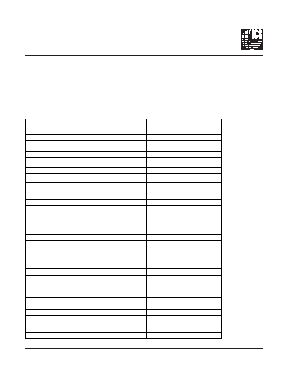
Absolute Maximum Ratings
Supply Voltage . . . . . . . . . . . . . . . . . . . . . . . . . 4.0 V
Logic Inputs . . . . . . . . . . . . . . . . . . . . . . . . . . . GND –0.5 V to VDD +0.5 V
Ambient Operating Temperature . . . . . . . . . . 0°C to +70°C
Storage Temperature . . . . . . . . . . . . . . . . . . . . –65°C to +150°C
Stresses above those listed under
Absolute Maximum Ratings may cause permanent damage to the device. These
ratings are stress specifications only and functional operation of the device at these or any other conditions above those
listed in the operational sections of the specifications is not implied. Exposure to absolute maximum rating conditions
for extended periods may affect product reliability.
Parameters
Symbol
Min
Max
Unit
Supply Voltage
VDD
3.135
3.465
V
Refclk Input cycle time
tCYCLE,IN
10
40
ns
Input cycle-to-cycle Jitter
tJ,IN
-250
ps
Input Duty cycle over 10k cycles
DCIN
40%
60%
tCYCLE
Input frequency of modulation
Fm,in
30
33
kHz
Modulation index
PM,IN
0.25
0.5
%
Phase detector input cycle time at PDclk/M & Synclk/N
tCYCLE,PD
30
100
ns
Initial phase error at phase detector inputs
Terr,init
-0.5
0.5
tCYCLE,PD
Phase detector input duty cycle over 10k cycles
DCIN,PD
25%
75%
tCYCLE,PD
Input rise & fall times ( measured at 20%-80% of input voltage) for
PDCLK/M & SYNCLK/N,&REfCLK
TIR,TIF
-1
ns
Input capacitance at PDCLK/M,Synclk/N,&REFCLK
CIN,PD
-7
pF
Input Capacitance matching at PCLK/M & SYNCLK/N
DCIN,PD
-0.5
pF
Input capacitance at CMOS pins
CIN,CMOS
-10
pF
Input (CMOS) signal low voltage
VIL
-0.3
Vdd
Input (CMOS) signal high voltage
VIH
0.7
-
Vdd
REFCLK input low voltage
VIL,R
-
0.3
Vddi,R
REFCLK input high voltage
VIH,R
0.7
-
Vddi,R
Input signal low voltage for PD inputs and STOP
VIL,PD
-
0.3
Vddi,PD
Input signal high voltage for PD inputs and STOP
VIH,PD
0.7
-
Vddi,PD
Input supply referance for REFCLK
VDD,IR
1.3
3.465
V
Input supply referance vfor PD inputs
VDDI,PD
1.3
3.465
V
Phase detector phase error for distributed loop measured at
PDCLK/M & SYNCLK/N(rising
tERR,PD
-100
100
ps
Cycle cycle time
tCYCLE
2.5
3.75
ns
Cycle-to-cycle jitter at Busclk/BUSCLKB (533 MHz)
tJ
-40
ps
Total jitter over 1 - 6 cycles (533MHz)
tJ
-30
ps
Phase aligner, phase step size (BSCLK/BUSCLKB)
tSTEP
1-
ps
PLL out put phase error when tracking SSC
tERR,SSC
-100
100
ps
Out put crossing-point voltage
VX
1.3
1.8
V
Output voltage swing
VCOS
0.4
0.6
V
Output high voltage
VH
-2
V
Out put duty cycle over 10k cycle
DC
40%
60%
tCYCLE
Output cycle -to-cycle duty cycle error
tDC,ERR
-50
ps
Output rise & fall times ( measured at 20%-80% of output voltage)
tCR,tCF
300
500
psd
Difference between rise and fall times on a single device(20%-80%)
tCR,CF
-100
ps
Opearting Supply Current
IDD
150
mA
Electrical Characteristics-input/supply/Outputs
相關(guān)PDF資料 |
PDF描述 |
|---|---|
| 9212AF-13LF | 533.3 MHz, PROC SPECIFIC CLOCK GENERATOR, PDSO24 |
| 9213100054 | PROXIMITY SENSOR-PHOTOELECTRIC, RECTANGULAR |
| 9213669104 | PROXIMITY SENSOR-PHOTOELECTRIC, RECTANGULAR |
| 9214711014 | PROXIMITY SENSOR-PHOTOELECTRIC, RECTANGULAR |
| 9214DGLF-T | 9214 SERIES, PLL BASED CLOCK DRIVER, 4 TRUE OUTPUT(S), 0 INVERTED OUTPUT(S), PDSO28 |
相關(guān)代理商/技術(shù)參數(shù) |
參數(shù)描述 |
|---|---|
| 9212AF-13LFT-IN0 | 制造商:Integrated Device Technology Inc 功能描述:RAMBUS CLOCK GENERATOR, SSOP24 - Tape and Reel |
| 9212BIM9200SERIES | 制造商:未知廠家 制造商全稱:未知廠家 功能描述:BOX POLYSTYRENE |
| 9212C | 制造商:Apex Tool Group 功能描述:PAIR OF REPLACEMENT JAWS, CENTER CUT, FOR 9290C PNEUMATIC CUTTER |
| 9212D | 功能描述:WR RAT DBL BX 12MMX13MM 制造商:apex tool group 系列:* 零件狀態(tài):在售 標(biāo)準(zhǔn)包裝:1 |
| 9212E | 制造商:Excelta Corporation 功能描述:Five Star 5" Carbon Steel Oval Relieved Semi-flush Cutter - 18 AWG Capacity soft wire - Made in USA |
發(fā)布緊急采購(gòu),3分鐘左右您將得到回復(fù)。