- 您現在的位置:買賣IC網 > PDF目錄24693 > 934054540127 (NXP SEMICONDUCTORS) 21 A, 55 V, 0.075 ohm, N-CHANNEL, Si, POWER, MOSFET, TO-220AB PDF資料下載
參數資料
| 型號: | 934054540127 |
| 廠商: | NXP SEMICONDUCTORS |
| 元件分類: | JFETs |
| 英文描述: | 21 A, 55 V, 0.075 ohm, N-CHANNEL, Si, POWER, MOSFET, TO-220AB |
| 封裝: | PLASTIC, SC-46, 3 PIN |
| 文件頁數: | 2/8頁 |
| 文件大小: | 65K |
| 代理商: | 934054540127 |
Philips Semiconductors
Product specification
TrenchMOS
transistor
PHP21N06T
Standard level FET
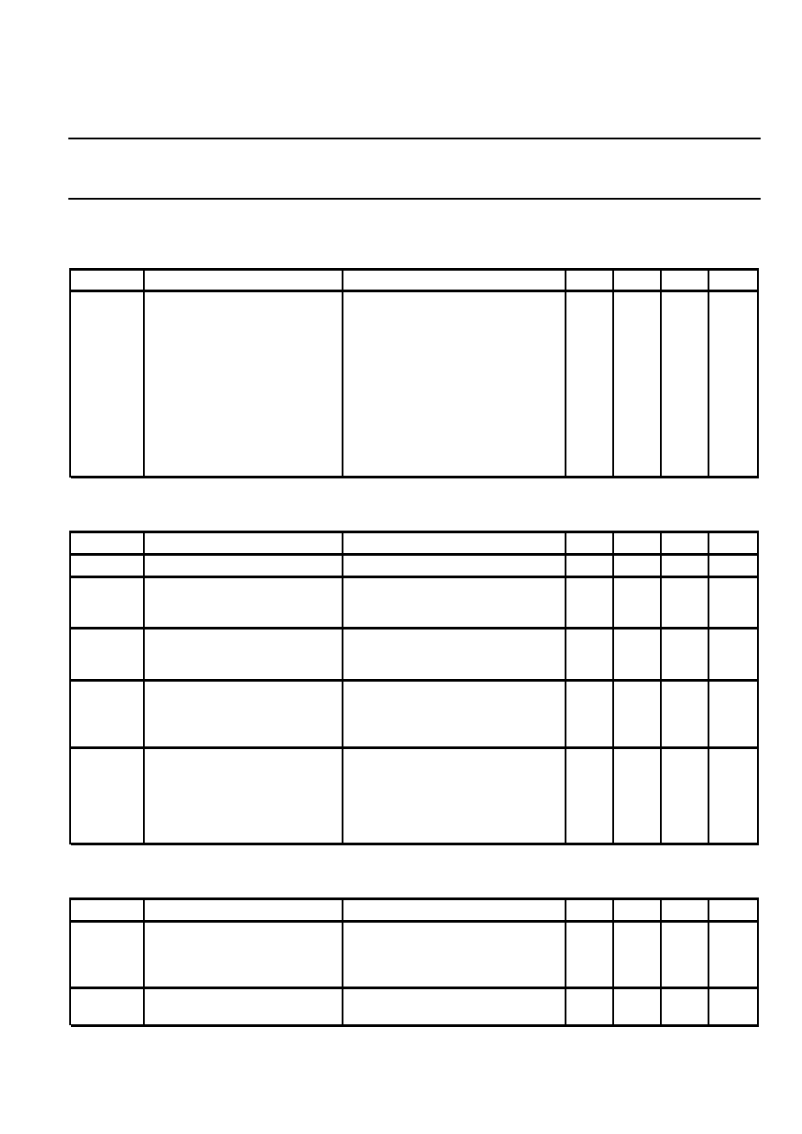
STATIC CHARACTERISTICS
T
j= 25C
unless otherwise specified
SYMBOL
PARAMETER
CONDITIONS
MIN.
TYP.
MAX.
UNIT
V
(BR)DSS
Drain-source breakdown
V
GS = 0 V; ID = 0.25 mA;
55
-
V
voltage
T
j = -55C
50
-
V
GS(TO)
Gate threshold voltage
V
DS = VGS; ID = 1 mA
2.0
3.0
4.0
V
T
j = 175C
1.0
-
V
T
j = -55C
-
4.4
I
DSS
Zero gate voltage drain current
V
DS = 55 V; VGS = 0 V;
-
0.05
10
A
T
j = 175C
-
500
A
I
GSS
Gate source leakage current
V
GS = ±10 V; VDS = 0 V
-
0.04
1
A
T
j = 175C
-
20
A
±V
(BR)GSS
Gate source breakdown voltage I
G = ±1 mA;
16
-
V
R
DS(ON)
Drain-source on-state
V
GS = 10 V; ID = 10 A
-
60
75
m
resistance
T
j = 175C
-
157
m
DYNAMIC CHARACTERISTICS
T
mb = 25C unless otherwise specified
SYMBOL
PARAMETER
CONDITIONS
MIN.
TYP.
MAX.
UNIT
g
fs
Forward transconductance
V
DS = 25 V; ID = 10 A
1
-
S
Q
g(tot)
Total gate charge
I
D = 20 A; VDD = 44 V; VGS = 10 V
-
13
-
nC
Q
gs
Gate-source charge
-
4
-
nC
Q
gd
Gate-drain (Miller) charge
-
5
-
nC
C
iss
Input capacitance
V
GS = 0 V; VDS = 25 V; f = 1 MHz
-
365
500
pF
C
oss
Output capacitance
-
110
135
pF
C
rss
Feedback capacitance
-
60
85
pF
t
d on
Turn-on delay time
V
DD = 30 V; ID = 10 A;
-
9
14
ns
t
r
Turn-on rise time
V
GS = 10 V; RG = 10
-
1621ns
t
d off
Turn-off delay time
Resistive load
-
14
25
ns
t
f
Turn-off fall time
-
13
20
ns
L
d
Internal drain inductance
Measured from contact screw on
-
3.5
-
nH
tab to centre of die
L
d
Internal drain inductance
Measured from drain lead 6 mm
-
4.5
-
nH
from package to centre of die
L
s
Internal source inductance
Measured from source lead 6 mm
-
7.5
-
nH
from package to source bond pad
REVERSE DIODE LIMITING VALUES AND CHARACTERISTICS
T
j = 25C unless otherwise specified
SYMBOL
PARAMETER
CONDITIONS
MIN.
TYP.
MAX.
UNIT
I
DR
Continuous reverse drain
-
21
A
current
I
DRM
Pulsed reverse drain current
-
84
A
V
SD
Diode forward voltage
I
F = 19.7 A; VGS = 0 V
-
0.95
1.2
V
t
rr
Reverse recovery time
I
F = 19.7 A; -dIF/dt = 100 A/s;
-
32
-
ns
Q
rr
Reverse recovery charge
V
GS = -10 V; VR = 30 V
-
0.12
-
C
December 1997
2
Rev 1.100
相關PDF資料 |
PDF描述 |
|---|---|
| 934054570118 | 19 A, 55 V, 0.075 ohm, N-CHANNEL, Si, POWER, MOSFET |
| 934054560127 | 19 A, 55 V, 0.075 ohm, N-CHANNEL, Si, POWER, MOSFET, TO220-AB |
| 934055349118 | 19 A, 55 V, 0.075 ohm, N-CHANNEL, Si, POWER, MOSFET |
| 05G4B48 | Silicon Diffused Type Rectifier Stack |
| 934054590135 | 4.9 A, 55 V, 0.04 ohm, N-CHANNEL, Si, POWER, MOSFET |
相關代理商/技術參數 |
參數描述 |
|---|---|
| 934054713215 | 制造商:NXP Semiconductors 功能描述:SUB ONLY TXSTR |
| 934054900215 | 制造商:NXP Semiconductors 功能描述:SUB ONLY TXSTR SGNL |
| 934054930215 | 制造商:NXP Semiconductors 功能描述:Diode Schottky 40V 0.2A 3-Pin TO-236AB T/R |
| 934054945115 | 制造商:NXP Semiconductors 功能描述:Diode Switching 100V 0.25A 2-Pin SOD-323 T/R |
| 934055092127 | 制造商:NXP Semiconductors 功能描述:H-OUT #7460 |
發(fā)布緊急采購,3分鐘左右您將得到回復。