- 您現(xiàn)在的位置:買賣IC網(wǎng) > PDF目錄24776 > 935063300118 (NXP SEMICONDUCTORS) LV/LV-A/LVX/H SERIES, DUAL POSITIVE EDGE TRIGGERED D FLIP-FLOP, COMPLEMENTARY OUTPUT, PDSO14 PDF資料下載
參數(shù)資料
| 型號: | 935063300118 |
| 廠商: | NXP SEMICONDUCTORS |
| 元件分類: | 鎖存器 |
| 英文描述: | LV/LV-A/LVX/H SERIES, DUAL POSITIVE EDGE TRIGGERED D FLIP-FLOP, COMPLEMENTARY OUTPUT, PDSO14 |
| 封裝: | 3.90 MM, PLASTIC, MS-012AB, SOT-109-1, SO-14 |
| 文件頁數(shù): | 5/12頁 |
| 文件大?。?/td> | 135K |
| 代理商: | 935063300118 |

1999 Aug 05
2
Philips Semiconductors
Product specication
16-bit D-type transparent latch with 30
series
termination resistors; 5 V input/output tolerant; 3-state
74LVC162373A;
74LVCH162373A
FEATURES
ESD protection:
HBM EIA/JESD22-A114-A
exceeds 2000 V
MM EIA/JESD22-A115-A
exceeds 200 V
5 V tolerant input/output for
interfacing with 5 V logic
Wide supply voltage range of
1.2 to 3.6 V
Complies with JEDEC standard
no. 8-1A
CMOS low power consumption
MULTIBYTE flow-through
standard pin-out architecture
Low inductance multiple power and
ground pins for minimum noise and
ground bounce
Direct interface with TTL levels
All data inputs have bus hold
(74LVCH162373A only)
High impedance when VCC =0
Power off disables outputs,
permitting live insertion.
DESCRIPTION
The 74LVC(H)162373A is a 16-bit D-type transparent latch featuring separate
D-type inputs for each latch and 3-state outputs for bus oriented applications.
One latch enable (LE) input and one output enable (OE) are provide for each
octal. Inputs can be driven from either 3.3 or 5 V devices. In 3-state operation,
outputs can handle 5 V. These features allow the use of these devices in a
mixed 3.3 and 5 V environment.
The 74LVC(H)162373 consists of 2 sections of eight D-type transparent latches
with 3-state true outputs. When LE is HIGH, data at the Dn inputs enter the
latches. In this condition the latches are transparent, i.e. a latch output will
change each time its corresponding D-input changes.
When LE is LOW the latches store the information that was present at the
D-inputs a set-up time preceding the HIGH-to-LOW transition of LE.
When OE is LOW, the contents of the eight latches are available at the outputs.
When OE is HIGH, the outputs go to the high-impedance OFF-state.
Operation of the OE input does not affect the state off latches.
The 74LVCH162373A bus hold data inputs eliminates the need for external pull
up resistors to hold unused inputs.
The 74LVC(H)162373A is designed with 30
series termination resistors in
both HIGH and LOW output stages to reduce line noise.
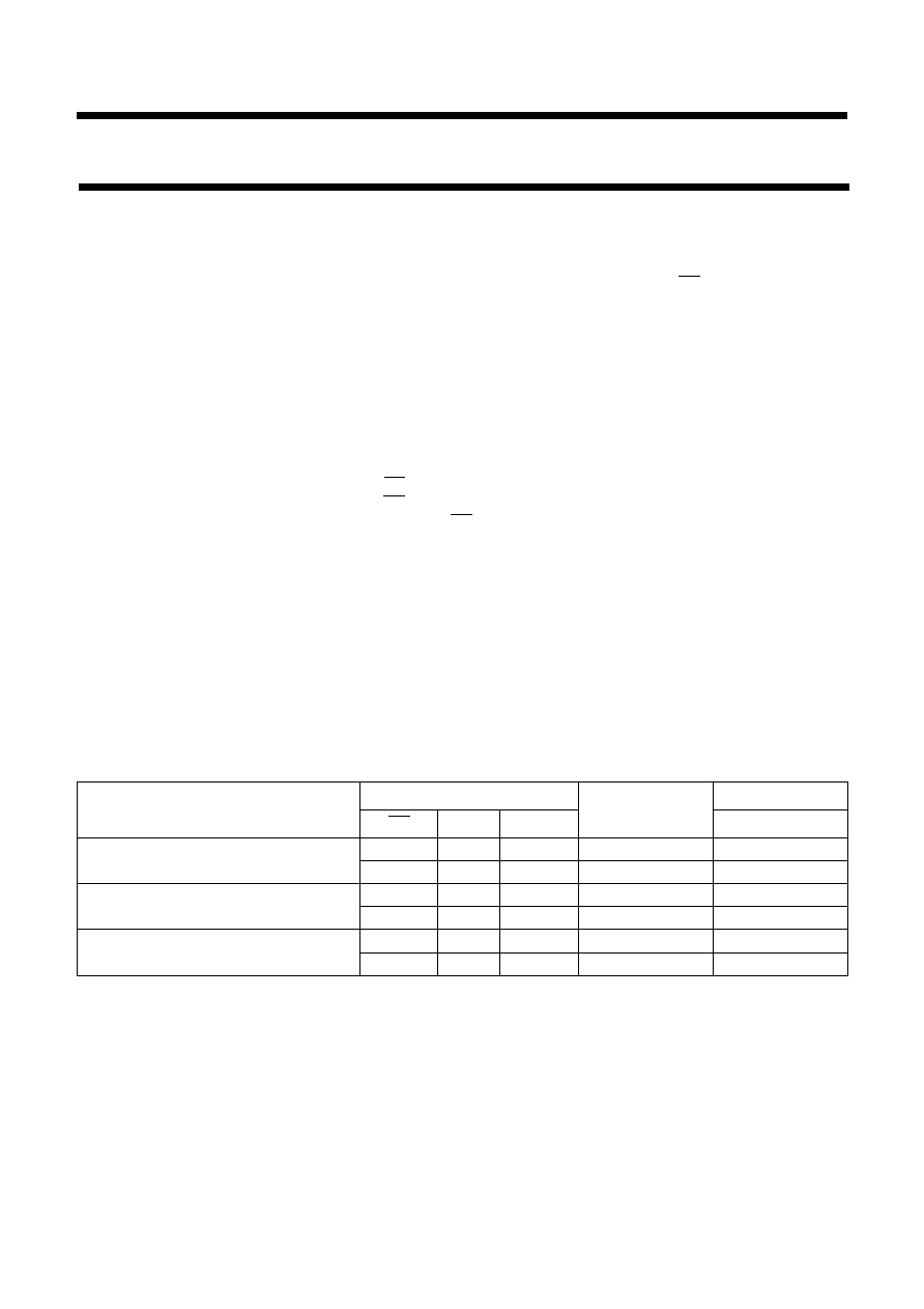
FUNCTION TABLE (per section of eight bits)
See note 1.
Note
1. H = HIGH voltage level;
h = HIGH voltage level one set-up time prior to the HIGH-to-LOW LE transition;
L = LOW voltage level;
l = LOW voltage level one set-up time prior to the HIGH-to-LOW LE transition;
Z = high-impedance OFF-state.
OPERATION MODES
INPUTS
INTERNAL
LATCHES
OUTPUTS
OE
LE
Dn
Q0 to Q7
Enable and read register
(transparent mode)
LH
L
LH
H
Latch and read register
LL
l
L
LL
h
H
Latch register and disable outputs
HL
l
L
Z
HL
h
H
Z
相關(guān)PDF資料 |
PDF描述 |
|---|---|
| 935171060118 | LVT SERIES, POSITIVE EDGE TRIGGERED D FLIP-FLOP, TRUE OUTPUT, PDSO20 |
| 935176350118 | LVT SERIES, POSITIVE EDGE TRIGGERED D FLIP-FLOP, TRUE OUTPUT, PDSO20 |
| 935176350112 | LVT SERIES, POSITIVE EDGE TRIGGERED D FLIP-FLOP, TRUE OUTPUT, PDSO20 |
| 935171050112 | LVT SERIES, POSITIVE EDGE TRIGGERED D FLIP-FLOP, TRUE OUTPUT, PDSO20 |
| 935171050118 | LVT SERIES, POSITIVE EDGE TRIGGERED D FLIP-FLOP, TRUE OUTPUT, PDSO20 |
相關(guān)代理商/技術(shù)參數(shù) |
參數(shù)描述 |
|---|---|
| 935066270112 | 制造商:NXP Semiconductors 功能描述:SUB ONLY I.C. |
| 93506EM8 | 制造商:undefined 功能描述: |
| 935079-000 | 制造商:TE Connectivity 功能描述:55A1841-16-MST4-9CS2275 - Cable Rools/Shrink Tubing |
| 935087-000 | 制造商:TE Connectivity 功能描述:301A511-51-05/164-0 - Bulk |
| 935087N001 | 制造商:TE Connectivity 功能描述:301A511-51-05/164-CS7092 制造商:TE Connectivity 功能描述:301A511-51-05/164-CS7092 - Bulk |
發(fā)布緊急采購,3分鐘左右您將得到回復(fù)。