- 您現(xiàn)在的位置:買賣IC網(wǎng) > PDF目錄24801 > 935260742118 (NXP SEMICONDUCTORS) LVC/LCX/Z SERIES, HEX 1-INPUT INVERT GATE, PDSO14 PDF資料下載
參數(shù)資料
| 型號: | 935260742118 |
| 廠商: | NXP SEMICONDUCTORS |
| 元件分類: | 門電路 |
| 英文描述: | LVC/LCX/Z SERIES, HEX 1-INPUT INVERT GATE, PDSO14 |
| 封裝: | 4.40 MM, PLASTIC, MO-153, SOT-402-1, TSSOP-14 |
| 文件頁數(shù): | 5/10頁 |
| 文件大小: | 98K |
| 代理商: | 935260742118 |
Philips Semiconductors
Product specification
74LVCU04A
Hex inverter
1998 Jul 29
4
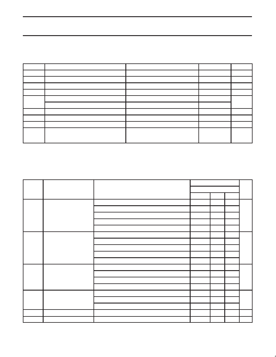
ABSOLUTE MAXIMUM RATINGS1
In accordance with the Absolute Maximum Rating System (IEC 134).
Voltages are referenced to GND (ground = 0V).
SYMBOL
PARAMETER
CONDITIONS
RATING
UNIT
VCC
DC supply voltage
–0.5 to +6.5
V
IIK
DC input diode current
VI t 0
–50
mA
VI
DC input voltage
Note 2
–0.5 to +6.5
V
IOK
DC output diode current
VO uVCC or VO t 0
"50
mA
VI/O
DC output voltage; output HIGH or LOW
Note NO TAG
–0.5 to VCC +0.5
V
VI/O
DC input voltage; output 3-State
Note NO TAG
–0.5 to 6.5
V
IO
DC output source or sink current
VO = 0 to VCC
"50
mA
IGND, ICC
DC VCC or GND current
"100
mA
Tstg
Storage temperature range
–65 to +150
°C
Power dissipation per package
PTOT
– plastic mini-pack (SO)
above +70
°C derate linearly with 8 mW/K
500
mW
– plastic shrink mini-pack (SSOP and TSSOP)
above +60
°C derate linearly with 5.5 mW/K
500
mW
NOTES:
1. Stresses beyond those listed may cause permanent damage to the device. These are stress ratings only and functional operation of the
device at these or any other conditions beyond those indicated under “recommended operating conditions” is not implied. Exposure to
absolute-maximum-rated conditions for extended periods may affect device reliability.
2. The input and output voltage ratings may be exceeded if the input and output current ratings are observed.
DC ELECTRICAL CHARACTERISTICS
Over recommended operating conditions. Voltages are referenced to GND (ground = 0V).
LIMITS
SYMBOL
PARAMETER
TEST CONDITIONS
Temp = -40
°C to +85°C
UNIT
MIN
TYP1
MAX
VCC = 1.2 V;VOL(max) = 0.5 V; IO = -100 mA
VCC
VCC = 2.0 V; VOL(max) = 0.5 V; IO = -100 mA
1.2
VIH
HIGH level Input voltage
VCC = 2.7 V; VOL(max) = 0.5 V; IO = -100 mA
1.8
V
VCC = 3.0 V; VOL(max) = 0.5 V; IO = -100 mA
2.0
VCC = 3.6 V; VOL(max) = 0.5 V; IO = -100 mA
2.4
VCC = 1.2 V; VOH(min) = VCC – 0.5 V; IO = 100 mA
GND
VCC = 2.0 V; VOH(min) = VCC – 0.5 V; IO = 100 mA
0.6
VIL
LOW level Input voltage
VCC = 2.7 V; VOH(min) = VCC – 0.5 V; IO = 100 mA
0.6
V
VCC = 3.0 V; VOH(min) = VCC – 0.5 V; IO = 100 mA
1.0
VCC = 3.6 V; VOH(min) = VCC – 0.5 V; IO = 100 mA
1.2
VCC = 2.7 V; VCC or GND; IO = -12 mA
VCC*0.5
VO
HIGH level output voltage
VCC = 3.0 V; VCC or GND; IO = -100mA
VCC*0.2
VCC
V
VOH
HIGH level output voltage
VCC = 3.0 V; VCC or GND; IO = -12 mA
VCC*0.6
V
VCC = 3.0 V; VCC or GND; IO = -24 mA
VCC*1.0
VCC = 2.7 V; VCC or GND; IO = 12 mA
0.40
VOL
LOW level output voltage
VCC = 3.0 V; VCC or GND; 12mA; IO = 100A
0.20
V
VCC = 3.0 V; VCC or GND; IO = 24mA
0.55
I
Input leakage current
VCC =3 6V; 55VorGND; Not for I/O pins
"01
"5
A
II
Input leakage current
VCC = 3.6 V; 5.5 V or GND; Not for I/O pins
"0.1
"5
A
ICC
Quiescent supply current
VCC = 3.6 V; VCC or GND; IO = 0
0.1
10
A
NOTE:
1. All typical values are at VCC = 3.3V and Tamb = 25°C.
相關(guān)PDF資料 |
PDF描述 |
|---|---|
| 935260740112 | LVC/LCX/Z SERIES, HEX 1-INPUT INVERT GATE, PDSO14 |
| 935260741118 | LVC/LCX/Z SERIES, HEX 1-INPUT INVERT GATE, PDSO14 |
| 935260740118 | LVC/LCX/Z SERIES, HEX 1-INPUT INVERT GATE, PDSO14 |
| 935260742112 | LVC/LCX/Z SERIES, HEX 1-INPUT INVERT GATE, PDSO14 |
| 0725 | 30 A, MODULAR TERMINAL BLOCK |
相關(guān)代理商/技術(shù)參數(shù) |
參數(shù)描述 |
|---|---|
| 935261069122 | 制造商:NXP Semiconductors 功能描述:IC SECURITY TRANSPONDER PLLMC |
| 935262025112 | 制造商:NXP Semiconductors 功能描述:SUB ONLY IC |
| 935262217118 | 制造商:NXP Semiconductors 功能描述:Real Time Clock Serial 8-Pin SO T/R |
| 935264217557 | 制造商:NXP Semiconductors 功能描述:SUB ONLY IC |
| 935267356112 | 制造商:NXP Semiconductors 功能描述:IC TEA1507PN |
發(fā)布緊急采購,3分鐘左右您將得到回復(fù)。