- 您現(xiàn)在的位置:買(mǎi)賣(mài)IC網(wǎng) > PDF目錄24807 > 935262800112 (NXP SEMICONDUCTORS) ALVC/VCX/A SERIES, 18-BIT REGISTERED TRANSCEIVER, TRUE OUTPUT, PDSO56 PDF資料下載
參數(shù)資料
| 型號(hào): | 935262800112 |
| 廠(chǎng)商: | NXP SEMICONDUCTORS |
| 元件分類(lèi): | 總線(xiàn)收發(fā)器 |
| 英文描述: | ALVC/VCX/A SERIES, 18-BIT REGISTERED TRANSCEIVER, TRUE OUTPUT, PDSO56 |
| 封裝: | PLASTIC, SOT-364, TSSOP-56 |
| 文件頁(yè)數(shù): | 12/22頁(yè) |
| 文件大?。?/td> | 135K |
| 代理商: | 935262800112 |
第1頁(yè)第2頁(yè)第3頁(yè)第4頁(yè)第5頁(yè)第6頁(yè)第7頁(yè)第8頁(yè)第9頁(yè)第10頁(yè)第11頁(yè)當(dāng)前第12頁(yè)第13頁(yè)第14頁(yè)第15頁(yè)第16頁(yè)第17頁(yè)第18頁(yè)第19頁(yè)第20頁(yè)第21頁(yè)第22頁(yè)
1999 Oct 14
2
Philips Semiconductors
Product specication
18-bit universal bus transceiver with 30
termination resistor; 3-state
74ALVCH162601
FEATURES
Complies with JEDEC standard
no. 8-1A
CMOS low power consumption
Direct interface with TTL levels
MULTIBYTE flow-through
standard pin-out architecture
Low inductance multiple VCC and
ground pins for minimum noise and
ground bounce
All data inputs have bus hold
circuitry
Integrated 30 termination
resistors.
DESCRIPTION
The 74ALVCH162601 is an 18-bit universal transceiver featuring non-inverting
3-state bus compatible outputs in both send and receive directions. Data flow
in each direction is controlled by output enable (OEAB and OEBA), and clock
(CPAB and CPBA) inputs. For A-to-B data flow, the device operates in the
transparent mode when LEAB is HIGH. When LEAB is LOW, the A data is
latched if CPAB is held at a HIGH or LOW logic level. If LEAB is LOW, the A-bus
data is stored in the latch/flip-flop on the LOW-to-HIGH transition of CPAB.
When OEAB is LOW, the outputs are active. When OEAB is HIGH, the outputs
are in the high-impedance state. The clocks can be controlled with the
clock-enable inputs (CEBA/CEAB).
Data flow for B-to-A is similar to that of A-to-B but uses OEBA,LEBA and CPBA.
To ensure the high-impedance state during power-down, OEBA and OEAB
should be tied to VCC through a pull-up resistor, the minimum value of the
resistor is determined by the current-sinking/current-sourcing capability of the
driver.
The 74ALVCH162601 is designed with 30
series resistors in both HIGH or
LOW output stage.
Active bus hold circuitry is provided to hold unused or floating data inputs at
a valid logic level.
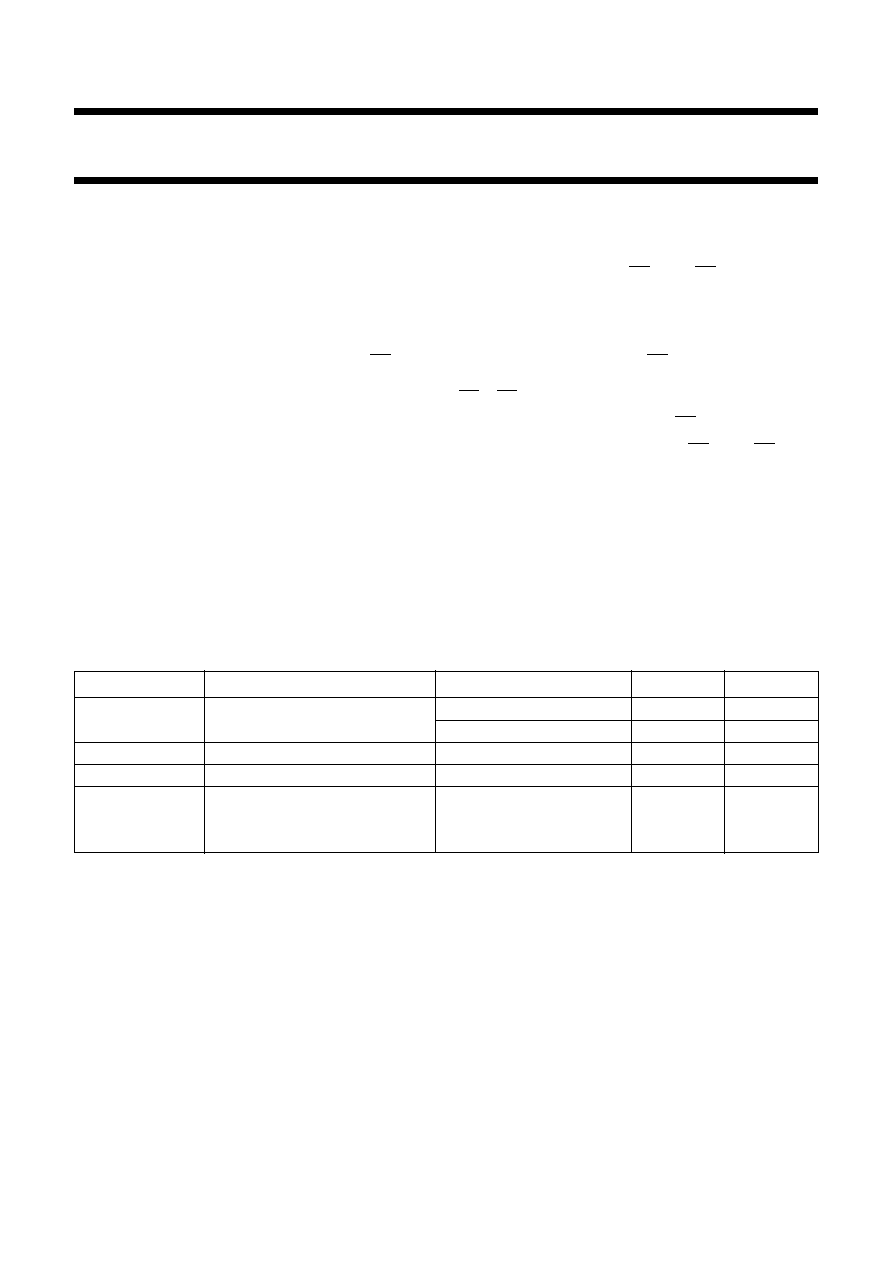
QUICK REFERENCE DATA
Ground = 0; Tamb =25 °C; tr =tf = 2.5 ns.
Notes
1. CPD is used to determine the dynamic power dissipation (PD in W).
PD =CPD × VCC2 × fi + ∑ (CL × VCC2 × fo) where:
fi = input frequency in MHz;
fo = output frequency in MHz;
∑ (CL × VCC2 × fo) = sum of outputs;
CL = output load capacitance in pF;
VCC = supply voltage in Volts.
2. The condition is VI = GND to VCC.
SYMBOL
PARAMETER
CONDITIONS
TYPICAL
UNIT
tPHL/tPLH
propagation delay An,Bn to Bn,An
CL = 30 pF; VCC = 2.5 V
4.0
ns
CL = 50 pF; VCC = 3.3 V
3.1
ns
CI/O
input/output capacitance
8.0
pF
CI
input capacitance
4.0
pF
CPD
power dissipation capacitance per
latch
notes 1 and 2
outputs enabled
21
pF
outputs disabled
3
pF
相關(guān)PDF資料 |
PDF描述 |
|---|---|
| 935262800118 | ALVC/VCX/A SERIES, 18 1-BIT REGISTERED TRANSCEIVER, TRUE OUTPUT, PDSO56 |
| 935262801118 | ALVC/VCX/A SERIES, DUAL 8-BIT REGISTERED TRANSCEIVER, TRUE OUTPUT, PDSO56 |
| 935262890112 | ATM/SONET/SDH SUPPORT CIRCUIT, PDSO16 |
| 935262890118 | ATM/SONET/SDH SUPPORT CIRCUIT, PDSO16 |
| 935262891026 | ATM/SONET/SDH SUPPORT CIRCUIT, UUC32 |
相關(guān)代理商/技術(shù)參數(shù) |
參數(shù)描述 |
|---|---|
| 935264217557 | 制造商:NXP Semiconductors 功能描述:SUB ONLY IC |
| 935267356112 | 制造商:NXP Semiconductors 功能描述:IC TEA1507PN |
| 935268081112 | 制造商:NXP Semiconductors 功能描述:SUB ONLY IC |
| 935268721125 | 制造商:NXP Semiconductors 功能描述:Buffer/Line Driver 1-CH Non-Inverting 3-ST CMOS 5-Pin TSSOP T/R |
| 935269304128 | 制造商:ST-Ericsson 功能描述:IC AUDIO CODEC W/TCH SCRN 48LQFP |
發(fā)布緊急采購(gòu),3分鐘左右您將得到回復(fù)。