- 您現(xiàn)在的位置:買(mǎi)賣(mài)IC網(wǎng) > PDF目錄24670 > 935263625026 (NXP SEMICONDUCTORS) LIQUID CRYSTAL DISPLAY DRIVER, U PDF資料下載
參數(shù)資料
| 型號(hào): | 935263625026 |
| 廠商: | NXP SEMICONDUCTORS |
| 元件分類(lèi): | 顯示驅(qū)動(dòng)器 |
| 英文描述: | LIQUID CRYSTAL DISPLAY DRIVER, U |
| 封裝: | DIE-40 |
| 文件頁(yè)數(shù): | 9/40頁(yè) |
| 文件大小: | 243K |
| 代理商: | 935263625026 |
第1頁(yè)第2頁(yè)第3頁(yè)第4頁(yè)第5頁(yè)第6頁(yè)第7頁(yè)第8頁(yè)當(dāng)前第9頁(yè)第10頁(yè)第11頁(yè)第12頁(yè)第13頁(yè)第14頁(yè)第15頁(yè)第16頁(yè)第17頁(yè)第18頁(yè)第19頁(yè)第20頁(yè)第21頁(yè)第22頁(yè)第23頁(yè)第24頁(yè)第25頁(yè)第26頁(yè)第27頁(yè)第28頁(yè)第29頁(yè)第30頁(yè)第31頁(yè)第32頁(yè)第33頁(yè)第34頁(yè)第35頁(yè)第36頁(yè)第37頁(yè)第38頁(yè)第39頁(yè)第40頁(yè)
1998 May 04
17
Philips Semiconductors
Product specication
Universal LCD driver for low multiplex
rates
PCF8566
7I2C-BUS DESCRIPTION
The I2C-bus is for 2-way, 2-line communication between
different ICs or modules. The two lines are a serial data
line (SDA) and a serial clock line (SCL). Both lines must be
connected to a positive supply via a pull-up resistor when
connected to the output stages of a device. Data transfer
may be initiated only when the bus is not busy.
7.1
Bit transfer
One data bit is transferred during each clock pulse.
The data on the SDA line must remain stable during the
HIGH period of the clock pulse as changes in the data line
at this time will be interpreted as control signals.
7.2
Start and stop conditions
Both data and clock lines remain HIGH when the bus is not
busy. A HIGH-to-LOW transition of the data line while the
clock is HIGH is defined as the START condition (S).
A LOW-to-HIGH transition of the data line while the clock
is HIGH is defined as the STOP condition (P).
7.3
System conguration
A device generating a message is a ‘transmitter’, a device
receiving a message is a ‘receiver’. The device that
controls the message is the ‘master’ and the devices which
are controlled by the master are the ‘slaves’.
7.4
Acknowledge
The number of data bytes transferred between the START
and STOP conditions from transmitter to receiver is not
limited. Each byte is followed by one acknowledge bit.
The acknowledge bit is a HIGH level put on the bus by the
transmitter whereas the master generates an extra
acknowledge related clock pulse. A slave receiver which is
addressed must generate an acknowledge after the
reception of each byte. Also a master must generate an
acknowledge after the reception of each byte that has
been clocked out of the slave transmitter. The device that
acknowledges has to pull down the SDA line during the
acknowledge clock pulse, so that the SDA line is stable
LOW during the HIGH period of the acknowledge related
clock pulse, set up and hold times must be taken into
account. A master receiver must signal an end of data to
the transmitter by not generating an acknowledge on the
last byte that has been clocked out of the slave. In this
event the transmitter must leave the data line HIGH to
enable the master to generate a STOP condition.
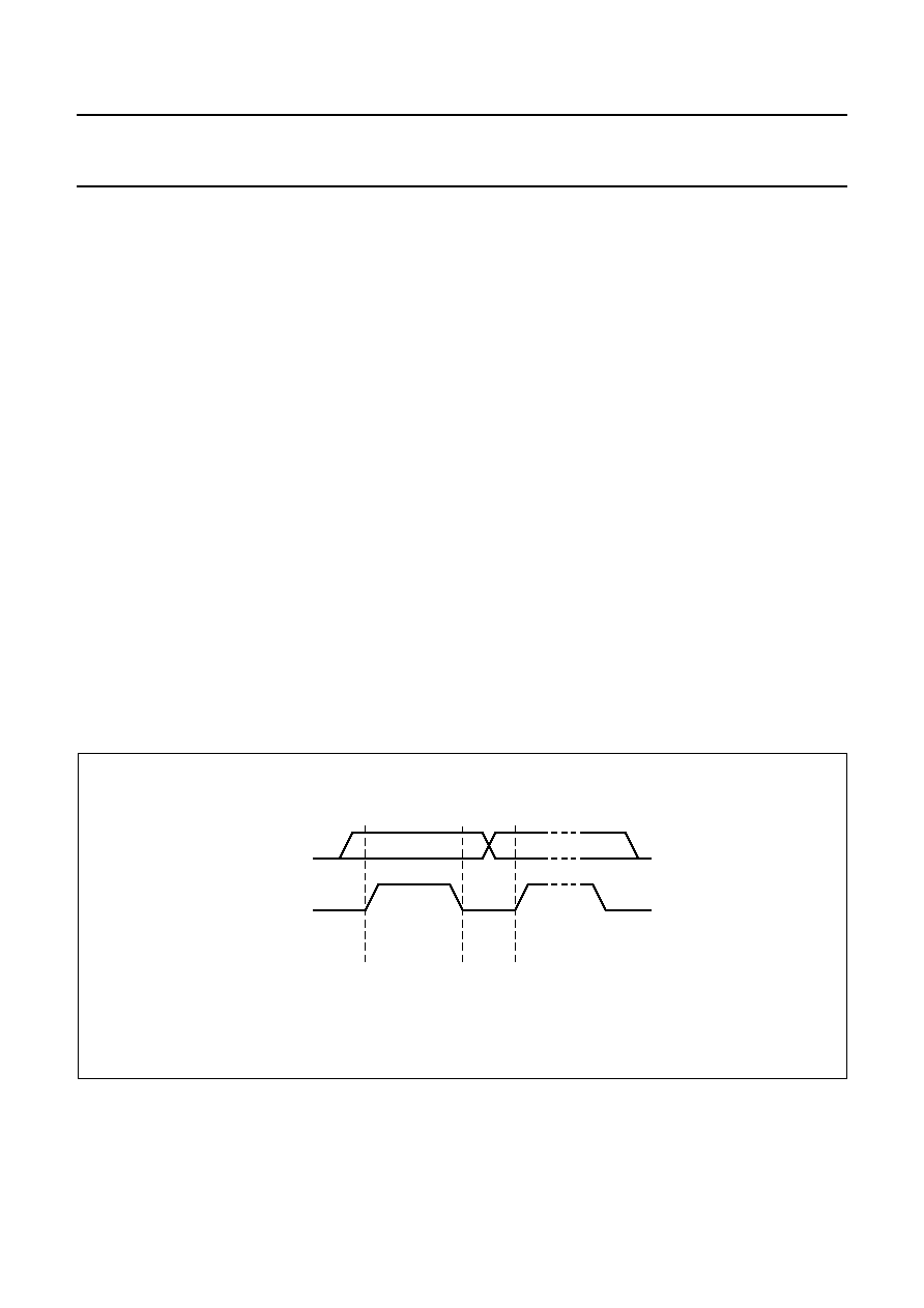
Fig.11 Bit transfer.
MBA607
data line
stable;
data valid
change
of data
allowed
SDA
SCL
相關(guān)PDF資料 |
PDF描述 |
|---|---|
| 0561168228 | PHOSPHOR BRONZE, TIN (40) FINISH, WIRE TERMINAL |
| 933876860602 | F/FAST SERIES, POSITIVE EDGE TRIGGERED D FLIP-FLOP, TRUE OUTPUT, PDIP16 |
| 933893120623 | F/FAST SERIES, POSITIVE EDGE TRIGGERED D FLIP-FLOP, TRUE OUTPUT, PDSO16 |
| 933893120602 | F/FAST SERIES, POSITIVE EDGE TRIGGERED D FLIP-FLOP, TRUE OUTPUT, PDSO16 |
| 933876880602 | F/FAST SERIES, ASYN NEGATIVE EDGE TRIGGERED 4-BIT UP BINARY COUNTER, PDIP14 |
相關(guān)代理商/技術(shù)參數(shù) |
參數(shù)描述 |
|---|---|
| 935264217557 | 制造商:NXP Semiconductors 功能描述:SUB ONLY IC |
| 935267356112 | 制造商:NXP Semiconductors 功能描述:IC TEA1507PN |
| 935268081112 | 制造商:NXP Semiconductors 功能描述:SUB ONLY IC |
| 935268721125 | 制造商:NXP Semiconductors 功能描述:Buffer/Line Driver 1-CH Non-Inverting 3-ST CMOS 5-Pin TSSOP T/R |
| 935269304128 | 制造商:ST-Ericsson 功能描述:IC AUDIO CODEC W/TCH SCRN 48LQFP |
發(fā)布緊急采購(gòu),3分鐘左右您將得到回復(fù)。