- 您現(xiàn)在的位置:買賣IC網(wǎng) > PDF目錄24813 > 935264043025 (NXP SEMICONDUCTORS) SPECIALTY TELECOM CIRCUIT, UUC13 PDF資料下載
參數(shù)資料
| 型號(hào): | 935264043025 |
| 廠商: | NXP SEMICONDUCTORS |
| 元件分類: | 通信及網(wǎng)絡(luò) |
| 英文描述: | SPECIALTY TELECOM CIRCUIT, UUC13 |
| 封裝: | DIE-13 |
| 文件頁(yè)數(shù): | 26/29頁(yè) |
| 文件大小: | 236K |
| 代理商: | 935264043025 |
第1頁(yè)第2頁(yè)第3頁(yè)第4頁(yè)第5頁(yè)第6頁(yè)第7頁(yè)第8頁(yè)第9頁(yè)第10頁(yè)第11頁(yè)第12頁(yè)第13頁(yè)第14頁(yè)第15頁(yè)第16頁(yè)第17頁(yè)第18頁(yè)第19頁(yè)第20頁(yè)第21頁(yè)第22頁(yè)第23頁(yè)第24頁(yè)第25頁(yè)當(dāng)前第26頁(yè)第27頁(yè)第28頁(yè)第29頁(yè)

2000 Mar 28
6
Philips Semiconductors
Product specication
Gigabit Ethernet/Fibre Channel
transimpedance amplier
TZA3043; TZA3043B
PIN diode bias voltage DREF
The transimpedance amplifier together with the PIN diode
determines the performance of an optical receiver for a
large extent. Especially how the PIN diode is connected to
the input and the layout around the input pin influence the
key parameters like sensitivity, the bandwidth and the
Power Supply Rejection Ratio (PSRR) of a
transimpedance amplifier. The total capacitance at the
input pin is critical to obtain the highest sensitivity. It should
be kept to a minimum by reducing the capacitance of the
PIN diode and the parasitics around the input pin. The
PIN diode should be placed very close to the IC to reduce
the parasitics. Because the capacitance of the PIN diode
depends on the reverse voltage across it, the reverse
voltage should be chosen as high as possible.
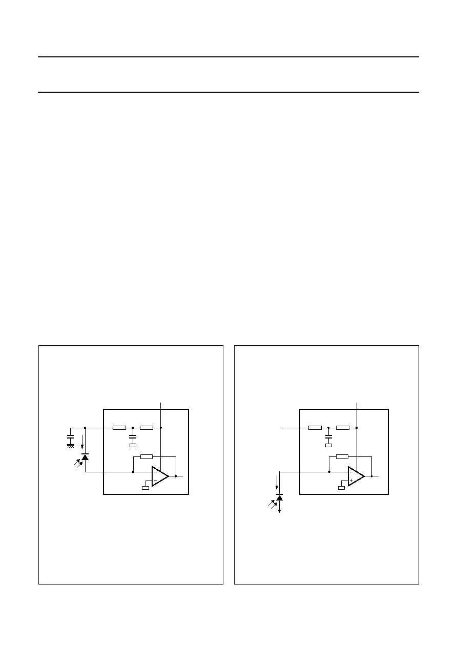
The PIN diode can be connected to the input in two ways
as shown in Figs 7 and 8. In Fig.7 the PIN diode is
connected between pins DREF and IPhoto. Pin DREF
provides an easy bias voltage for the PIN diode. The
voltage at DREF is derived from VCC by a low-pass filter.
The low-pass filter consisting of the internal resistors
R1, R2, C1 and the external capacitor C2 rejects the
supply voltage noise. The external capacitor C2 should be
equal or larger then 1 nF for a high PSRR.
The reverse voltage across the PIN diode is 4.18 V
(5
0.82 V) for 5 V supply or 2.48 V (3.3 0.82 V) for
3.3 V supply.
It is preferable to connect the cathode of the PIN diode to
a higher voltage then VCC when such a voltage source is
available on the board. In this case pin DREF can be left
unconnected. When a negative supply voltage is available,
the configuration in Fig.8 can be used. It should be noted
that in this case the direction of the signal current is
reversed compared to the Fig.7. Proper filtering of the bias
voltage for the PIN diode is essential to achieve the
highest sensitivity level.
MGU103
R1
125
R2
125
C1
10 pF
C2
1 nF
VCC
Ii
1
8
TZA3043
3
IPhoto
DREF
Fig.7
The PIN diode connected between the input
and pin DREF.
MGU104
R1
125
R2
125
C1
10 pF
VCC
1
8
TZA3043
3
IPhoto
DREF
Ii
negative supply voltage
Fig.8
The PIN diode connected between the input
and a negative supply voltage.
相關(guān)PDF資料 |
PDF描述 |
|---|---|
| 935263511026 | SPECIALTY TELECOM CIRCUIT, UUC13 |
| 935263510112 | SPECIALTY TELECOM CIRCUIT, PDSO8 |
| 08-130150-01 | OUTLINE EXTENDED PFC MINI 1/RU |
| 08-130150-01-A1 | OUTLINE EXTENDED PFC MINI 1/RU |
| 935264068118 | DUAL 2 LINE TO 1 LINE MULTIPLEXER, TRUE OUTPUT, PDSO14 |
相關(guān)代理商/技術(shù)參數(shù) |
參數(shù)描述 |
|---|---|
| 935264217557 | 制造商:NXP Semiconductors 功能描述:SUB ONLY IC |
| 935267356112 | 制造商:NXP Semiconductors 功能描述:IC TEA1507PN |
| 935268081112 | 制造商:NXP Semiconductors 功能描述:SUB ONLY IC |
| 935268721125 | 制造商:NXP Semiconductors 功能描述:Buffer/Line Driver 1-CH Non-Inverting 3-ST CMOS 5-Pin TSSOP T/R |
| 935269304128 | 制造商:ST-Ericsson 功能描述:IC AUDIO CODEC W/TCH SCRN 48LQFP |
發(fā)布緊急采購(gòu),3分鐘左右您將得到回復(fù)。