- 您現(xiàn)在的位置:買賣IC網(wǎng) > PDF目錄24813 > 935264404112 (NXP SEMICONDUCTORS) PLL BASED CLOCK DRIVER, 9 TRUE OUTPUT(S), 0 INVERTED OUTPUT(S), PDSO24 PDF資料下載
參數(shù)資料
| 型號(hào): | 935264404112 |
| 廠商: | NXP SEMICONDUCTORS |
| 元件分類: | 時(shí)鐘及定時(shí) |
| 英文描述: | PLL BASED CLOCK DRIVER, 9 TRUE OUTPUT(S), 0 INVERTED OUTPUT(S), PDSO24 |
| 封裝: | 4.40 MM, PLASTIC, MO-153, SOT-355-1, TSSOP-24 |
| 文件頁(yè)數(shù): | 6/10頁(yè) |
| 文件大小: | 79K |
| 代理商: | 935264404112 |

Philips Semiconductors
Product specification
PCK2509S
50–150 MHz 1:9 SDRAM clock driver
2001 Feb 02
5
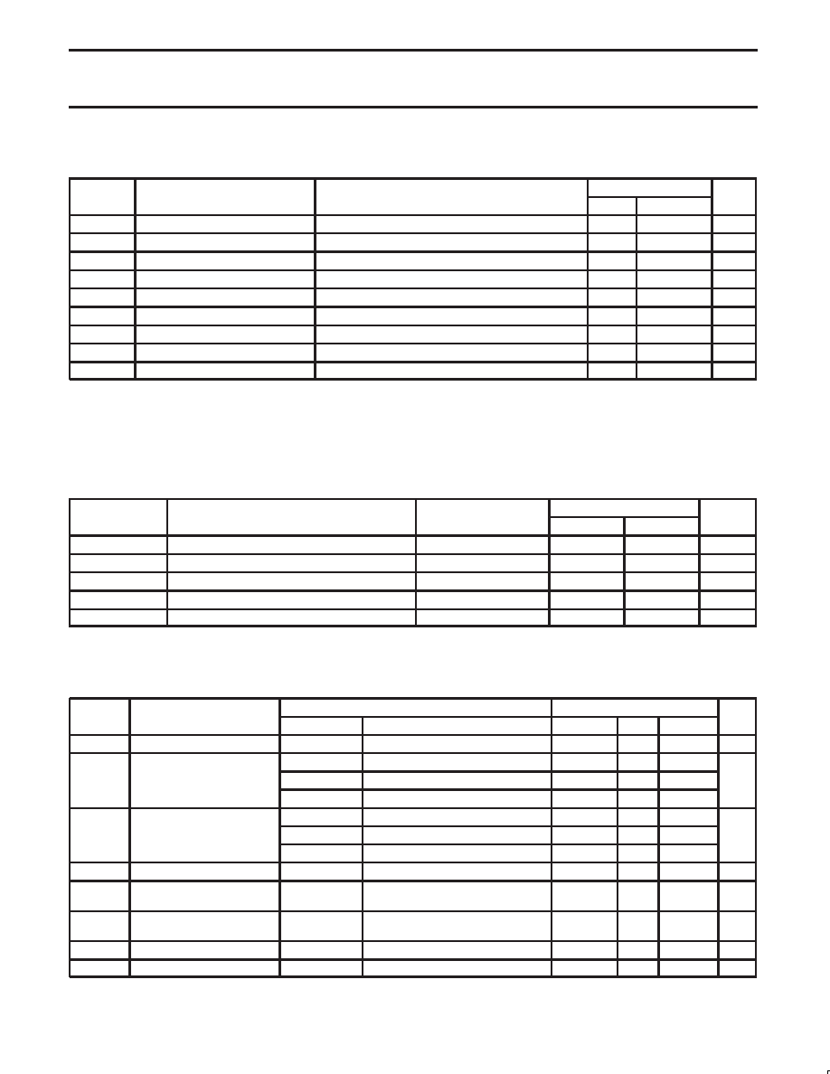
ABSOLUTE MAXIMUM RATINGS1
In accordance with the Absolute Maximum Rating System (IEC 134)
SYMBOL
PARAMETER
CONDITION
LIMITS
UNIT
SYMBOL
PARAMETER
CONDITION
MIN
MAX
UNIT
AVCC
Supply voltage range
Note 2
< VCC + 0.7
V
VCC
Supply voltage range
–0.5
+4.6
V
IIK
Input clamp current
VI < 0
–50
mA
VI
Input voltage range
Note 3
–0.5
6.5
V
IOK
Output clamp current
VO > VCC or VO < 0
±50
mA
VO
Output voltage range
Notes 3, 4
–0.5
VCC + 0.5
V
IO
DC output source or sink current
VO = 0 to VCC
±50
mA
TSTG
Storage temperature range
–65
+150
°C
PTOT
Power dissipation per package
700
mW
NOTES:
1. Stresses beyond those listed may cause permanent damage to the device. These are stress ratings only and functional operation of the
device at these or any other conditions beyond those indicated under “recommended operating conditions” is not implied. Exposure to
absolute-maximum-rated conditions for extended periods may affect device reliability.
2. AVCC must not exceed VCC
3. The input and output voltage ratings may be exceeded if the input and output current ratings are observed.
4. This value is limited to 4.6 V maximum.
RECOMMENDED OPERATING CONDITIONS1
SYMBOL
PARAMETER
CONDITIONS
LIMITS
UNIT
SYMBOL
PARAMETER
CONDITIONS
MIN
MAX
UNIT
VCC, AVCC
Supply voltage
3
3.6
V
VIH
HIGH level input voltage
2
V
VIL
LOW level input voltage
0.8
V
VI
Input voltage
0
VCC
V
Tamb
Operating ambient temperature range in free air
0
+70
°C
NOTE:
1. Unused inputs must be held high or low to prevent them from floating.
ELECTRICAL CHARACTERISTICS
Over recommended operating free-air temperature range (unless otherwise specified)
SYMBOL
PARAMETER
TEST CONDITIONS
LIMITS
UNIT
SYMBOL
PARAMETER
AVCC, VCC (V)
OTHER
MIN
TYP
MAX
UNIT
VIK
Input clamp voltage
3
II = –18 mA
–1.2
V
MIN to MAX
IOH = – 100 A
VCC – 0.2
VOH
HIGH level output voltage
3
IOH = – 12 mA
2.1
V
3
IOH = – 6 mA
2.4
MIN to MAX
IOL = 100 A
–
0.2
VOL
LOW level output voltage
3
IOL = 12 mA
–
0.8
V
3
IOL = 6 mA
–
0.55
II
Input current
3.6
VI = VCC or GND
±5
A
ICC
Quiescent supply current
3.6
VI = VCC or GND;
IO = 0, outputs: LOW or HIGH
10
A
ICC
Additional supply current per
input pin
3.3 to 3.6
One input at VCC – 0.6 V;
other inputs at VCC or GND
500
A
CI
Input capacitance
3.3
VI = VCC or GND
2.8
pF
CO
Output capacitance
3.3
VO= VCC or GND
5.4
pF
NOTE:
1. For ICCA and ICC vs. frequency, see Figures 3 and 4.
相關(guān)PDF資料 |
PDF描述 |
|---|---|
| 935264404118 | PLL BASED CLOCK DRIVER, 9 TRUE OUTPUT(S), 0 INVERTED OUTPUT(S), PDSO24 |
| 935264405112 | PLL BASED CLOCK DRIVER, 10 TRUE OUTPUT(S), 0 INVERTED OUTPUT(S), PDSO24 |
| 935264405118 | PLL BASED CLOCK DRIVER, 10 TRUE OUTPUT(S), 0 INVERTED OUTPUT(S), PDSO24 |
| 935264443112 | AVC SERIES, 16 1-BIT DRIVER, TRUE OUTPUT, PDSO48 |
| 935264443118 | AVC SERIES, 16 1-BIT DRIVER, TRUE OUTPUT, PDSO48 |
相關(guān)代理商/技術(shù)參數(shù) |
參數(shù)描述 |
|---|---|
| 935267356112 | 制造商:NXP Semiconductors 功能描述:IC TEA1507PN |
| 935268081112 | 制造商:NXP Semiconductors 功能描述:SUB ONLY IC |
| 935268721125 | 制造商:NXP Semiconductors 功能描述:Buffer/Line Driver 1-CH Non-Inverting 3-ST CMOS 5-Pin TSSOP T/R |
| 935269304128 | 制造商:ST-Ericsson 功能描述:IC AUDIO CODEC W/TCH SCRN 48LQFP |
| 935269544557 | 制造商:NXP Semiconductors 功能描述:SUB ONLY TDA9587-2US1-V1.3 |
發(fā)布緊急采購(gòu),3分鐘左右您將得到回復(fù)。