- 您現(xiàn)在的位置:買賣IC網(wǎng) > PDF目錄24813 > 935264405112 (NXP SEMICONDUCTORS) PLL BASED CLOCK DRIVER, 10 TRUE OUTPUT(S), 0 INVERTED OUTPUT(S), PDSO24 PDF資料下載
參數(shù)資料
| 型號(hào): | 935264405112 |
| 廠商: | NXP SEMICONDUCTORS |
| 元件分類: | 時(shí)鐘及定時(shí) |
| 英文描述: | PLL BASED CLOCK DRIVER, 10 TRUE OUTPUT(S), 0 INVERTED OUTPUT(S), PDSO24 |
| 封裝: | 4.40 MM, PLASTIC, MO-153, SOT-355-1, TSSOP-24 |
| 文件頁(yè)數(shù): | 3/10頁(yè) |
| 文件大小: | 95K |
| 代理商: | 935264405112 |

Philips Semiconductors
Product specification
PCK2510S
50–150 MHz 1:10 SDRAM clock driver
2
2001 Feb 02
853–2184 25550
FEATURES
Phase-Locked Loop Clock distribution for PC100/PC133 SDRAM
applications
Spread Spectrum clock compatible
Operating frequency 50 to 150 MHz
(t
phase error – jitter) at 100 to133 MHz = ±50 ps
Jitter (peak-peak) at 100 to 133 MHz = ± 80 ps
Jitter (cycle-cycle) at 100 to 133 MHz = 65 ps
Pin-to-pin skew < 200 ps
Available in plastic 24-Pin TSSOP
Distributes one clock input to one bank of ten outputs
External Feedback (FBIN) terminal Is used to synchronize the
outputs to the clock input
On-Chip series damping resistors
No external RC network required
Operates at 3.3 V
See page 8 for characteristic curves
DESCRIPTION
The PCK2510S is a high-performance, low-skew, low-jitter,
phase-locked loop (PLL) clock driver. It uses a PLL to precisely
align, in both frequency and phase, the feedback (FBOUT) output to
the clock (CLK) input signal. It is specifically designed for use with
synchronous DRAMs. The PCK2510S operates at 3.3 V VCC and is
input compatible with both 2.5 V and 3.3 V input voltage ranges. It
also provides integrated series damping resistors that make it ideal
for driving point-to-point loads.
One bank of ten outputs provides ten low-skew, low-jitter copies of
CLK. Output signal duty cycles are adjusted to 50 percent,
independent of the duty cycle at CLK. All outputs can be enabled or
disabled via a single output enable input. When the G input is high,
the outputs switch in phase and frequency with CLK; when the G
input is low, the outputs are disabled to the logic-low state.
Unlike many products containing PLLs, the PCK2510S does not
require external RC networks. The loop filter for the PLL is included
on-chip, minimizing component count, board space, and cost.
Because it is based on PLL circuitry, the PCK2510S requires a
stabilization time to achieve phase lock of the feedback signal to the
reference signal. This stabilization time is required, following power
up and application of a fixed-frequency, fixed-phase signal at CLK,
and following any changes to the PLL reference. The PLL can be
bypassed for test purposes by strapping AVCC to ground.
The PCK2510S is characterized for operation from 0
°C to +70 °C.
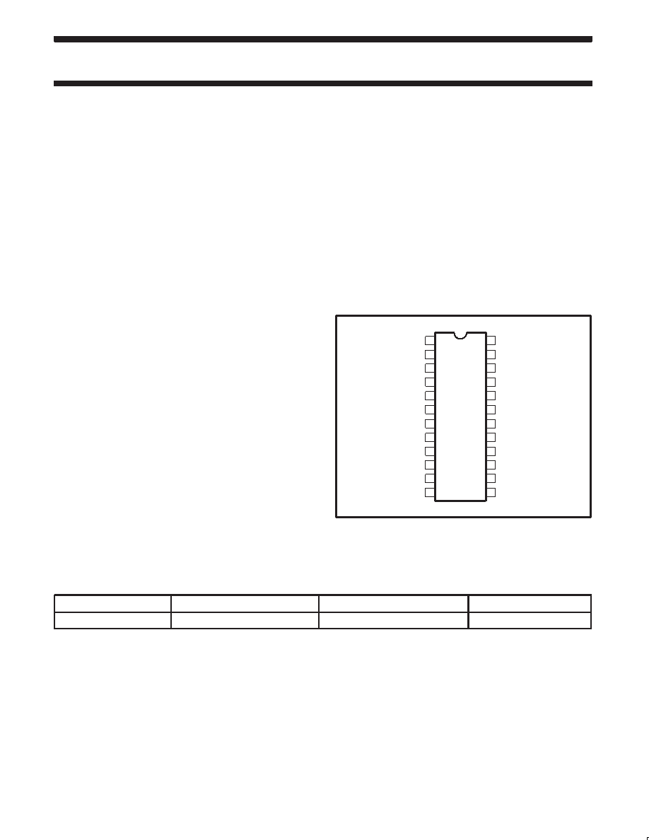
PIN CONFIGURATION
1
2
3
4
5
6
7
8
9
10
11
12
13
14
15
16
17
18
19
20
21
22
23
24
AGND
CLK
AVCC
VCC
1Y9
1Y0
1Y8
GND
1Y1
GND
1Y6
1Y2
1Y7
1Y5
GND
VCC
FBIN
GND
1Y3
1Y4
SW00382
VCC
G
FBOUT
ORDERING INFORMATION
PACKAGES
TEMPERATURE RANGE
ORDER CODE
DRAWING NUMBER
24-Pin Plastic TSSOP
0 to +70
°C
PCK2510SPW
SOT355-1
相關(guān)PDF資料 |
PDF描述 |
|---|---|
| 935264405118 | PLL BASED CLOCK DRIVER, 10 TRUE OUTPUT(S), 0 INVERTED OUTPUT(S), PDSO24 |
| 935264443112 | AVC SERIES, 16 1-BIT DRIVER, TRUE OUTPUT, PDSO48 |
| 935264443118 | AVC SERIES, 16 1-BIT DRIVER, TRUE OUTPUT, PDSO48 |
| 08-30-0110 | 156 KK Term RA Loose Brass 11Ckt |
| 935264444118 | AVC SERIES, 16 1-BIT TRANSCEIVER, TRUE OUTPUT, PDSO48 |
相關(guān)代理商/技術(shù)參數(shù) |
參數(shù)描述 |
|---|---|
| 935267356112 | 制造商:NXP Semiconductors 功能描述:IC TEA1507PN |
| 935268081112 | 制造商:NXP Semiconductors 功能描述:SUB ONLY IC |
| 935268721125 | 制造商:NXP Semiconductors 功能描述:Buffer/Line Driver 1-CH Non-Inverting 3-ST CMOS 5-Pin TSSOP T/R |
| 935269304128 | 制造商:ST-Ericsson 功能描述:IC AUDIO CODEC W/TCH SCRN 48LQFP |
| 935269544557 | 制造商:NXP Semiconductors 功能描述:SUB ONLY TDA9587-2US1-V1.3 |
發(fā)布緊急采購(gòu),3分鐘左右您將得到回復(fù)。