- 您現(xiàn)在的位置:買賣IC網(wǎng) > PDF目錄24826 > 935267419551 (NXP SEMICONDUCTORS) 1 CHANNEL(S), 1M bps, SERIAL COMM CONTROLLER, PQFP44 PDF資料下載
參數(shù)資料
| 型號: | 935267419551 |
| 廠商: | NXP SEMICONDUCTORS |
| 元件分類: | 微控制器/微處理器 |
| 英文描述: | 1 CHANNEL(S), 1M bps, SERIAL COMM CONTROLLER, PQFP44 |
| 封裝: | 10 X 10 MM, 1.75 MM HEIGHT, PLASTIC, SOT-307-2, QFP-44 |
| 文件頁數(shù): | 7/42頁 |
| 文件大?。?/td> | 249K |
| 代理商: | 935267419551 |
第1頁第2頁第3頁第4頁第5頁第6頁當(dāng)前第7頁第8頁第9頁第10頁第11頁第12頁第13頁第14頁第15頁第16頁第17頁第18頁第19頁第20頁第21頁第22頁第23頁第24頁第25頁第26頁第27頁第28頁第29頁第30頁第31頁第32頁第33頁第34頁第35頁第36頁第37頁第38頁第39頁第40頁第41頁第42頁

Philips Semiconductors
Product specification
SC28L91
3.3V–5.0V Universal Asynchronous
Receiver/Transmitter (UART)
2000 Sep 22
15
Unit
Max
Typ
Min
Parameter
Symbol
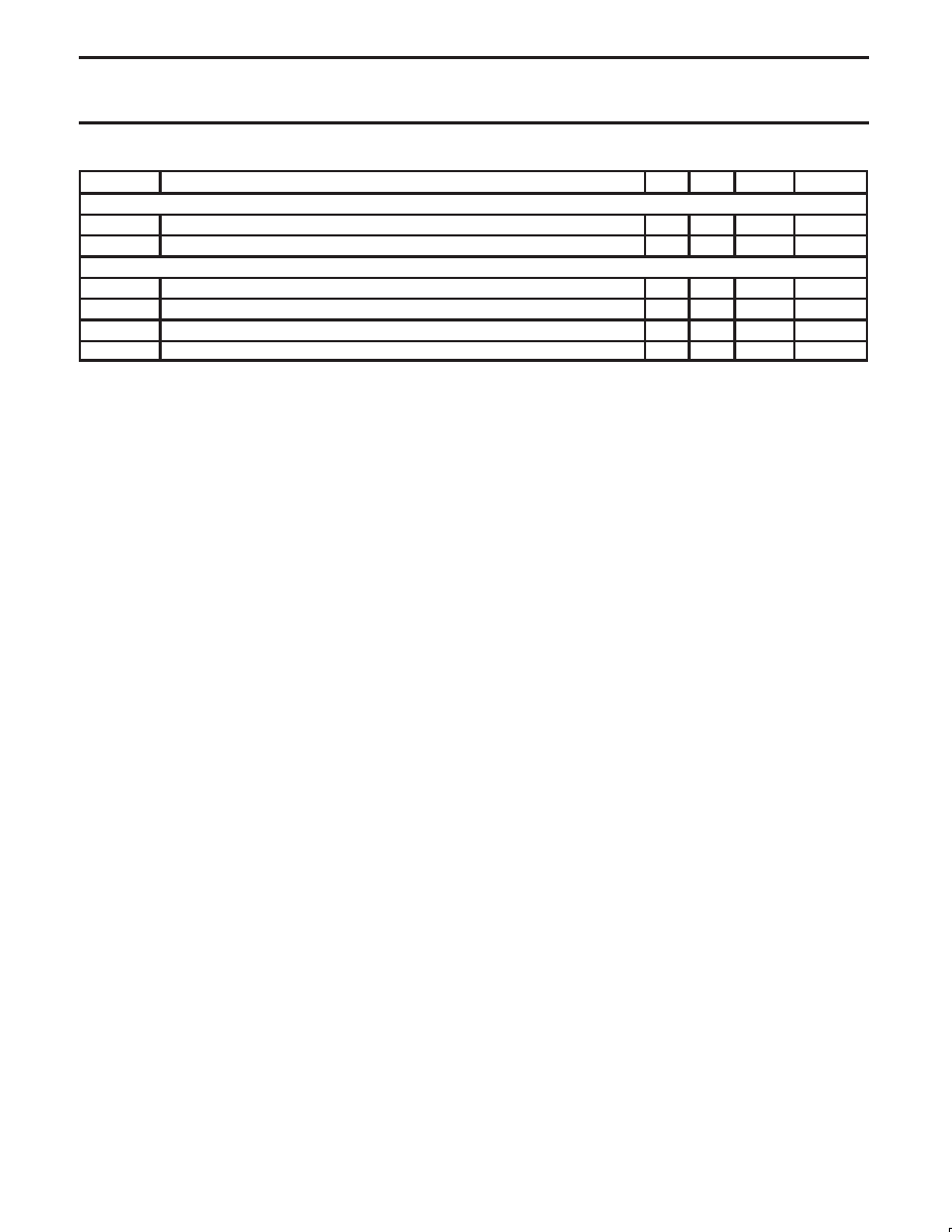
Receiver Timing, external clock (See Figure 13)
t*RXS
RxD data setup time to RxC high
50
10
ns
t*RXH
RxD data hold time from RxC high
50
10
ns
68000 or Motorola bus timing (See Figures 6, 7, 8)10
tDCR
DACKN Low (read cycle) from X1 High10
18
25
ns
tDCW
DACKN Low (write cycle) from X1 High
18
25
ns
tDAT
DACKN High impedance from CEN or IACKN High
10
15
ns
tCSC
CEN or IACKN setup time to X1 High for minimum DACKN cycle
15
10
ns
NOTES:
1. Parameters are valid over specified temperature and voltage range.
2. All voltage measurements are referenced to ground (GND). For testing, all inputs swing between 0.4 V and 3.0 V with a transition time of
5 ns maximum. For X1/CLK this swing is between 0.4 V and 0.8*VCC. All time measurements are referenced at input voltages of 0.8 V and
2.0 V and output voltages of 0.8 V and 2.0 V, as appropriate.
3. Test conditions for outputs: CL = 125 pF, except open drain outputs. Test conditions for open drain outputs: CL = 125 pF,
constant current source = 2.6 mA.
4. Typical values are the average values at +25
°C and 3.3 V.
5. Timing is illustrated and referenced to the WRN and RDN Inputs. Also, CEN may be the “strobing” input. CEN and RDN (also CEN and
WRN) are ORed internally. The signal asserted last initiates the cycle and the signal negated first terminates the cycle.
6. Guaranteed by characterization of sample units.
7. If CEN is used as the “strobing” input, the parameter defines the minimum High times between one CEN and the next. The RDN signal must
be negated for tRWD to guarantee that any status register changes are valid.
8. Minimum frequencies are not tested but are guaranteed by design.
9. Clocks for 1X mode should maintain a 60/40 duty cycle or better.
10. Minimum DACKN time is tDCR = tDSC + tDCR + two positive edges of the X1 clock. For faster bus cycles, the 80XXX bus timing may be used
while in the 68XXX mode. It is not necessary to wait for DACKN to insure the proper operation of the SC28C91. In all cases the data will be
written to the SC28L91 on the falling edge of DACKN or the rise of CEN. The fall of CEN initializes the bus cycle. The rise of CEN ends the
bus cycle. DACKN low or CEN high completes the write cycle.
相關(guān)PDF資料 |
PDF描述 |
|---|---|
| 935267418529 | 1 CHANNEL(S), 1M bps, SERIAL COMM CONTROLLER, PQCC44 |
| 935267418512 | 1 CHANNEL(S), 1M bps, SERIAL COMM CONTROLLER, PQCC44 |
| 935267419557 | 1 CHANNEL(S), 1M bps, SERIAL COMM CONTROLLER, PQFP44 |
| 08-M150-KIT-FEC | IMPACT PRINTER KIT |
| 08-M160-KIT-FEC | IMPACT PRINTER KIT |
相關(guān)代理商/技術(shù)參數(shù) |
參數(shù)描述 |
|---|---|
| 935268081112 | 制造商:NXP Semiconductors 功能描述:SUB ONLY IC |
| 935268721125 | 制造商:NXP Semiconductors 功能描述:Buffer/Line Driver 1-CH Non-Inverting 3-ST CMOS 5-Pin TSSOP T/R |
| 935269304128 | 制造商:ST-Ericsson 功能描述:IC AUDIO CODEC W/TCH SCRN 48LQFP |
| 935269544557 | 制造商:NXP Semiconductors 功能描述:SUB ONLY TDA9587-2US1-V1.3 |
| 935269987557 | 制造商:NXP Semiconductors 功能描述:SUB ONLY TDA9587-1US1-V1.8 SUBBED TO 935269987557 |
發(fā)布緊急采購,3分鐘左右您將得到回復(fù)。