- 您現(xiàn)在的位置:買賣IC網(wǎng) > PDF目錄42387 > 93AA46T-I/MS 64 X 16 MICROWIRE BUS SERIAL EEPROM, PDSO8 PDF資料下載
參數(shù)資料
| 型號: | 93AA46T-I/MS |
| 元件分類: | PROM |
| 英文描述: | 64 X 16 MICROWIRE BUS SERIAL EEPROM, PDSO8 |
| 封裝: | PLASTIC, MSOP-8 |
| 文件頁數(shù): | 12/20頁 |
| 文件大?。?/td> | 510K |
| 代理商: | 93AA46T-I/MS |
93XX46, 93XX46A/B
DS21749A-page 2
2002 Microchip Technology Inc.
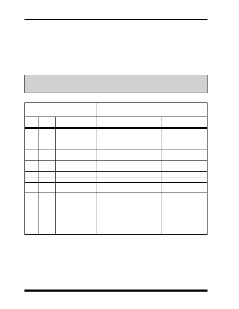
1.0
ELECTRICAL CHARACTERISTICS
Absolute Maximum Ratings
V
CC.............................................................................................................................................................................6.5V
All inputs and outputs w.r.t. V
SS ......................................................................................................... -0.6V to VCC +1.0V
Storage temperature ...............................................................................................................................-65°C to +150°C
Ambient temp. with power applied ..........................................................................................................-40°C to +125°C
ESD protection on all pins
......................................................................................................................................................≥ 4kV
DC C
HARACTERISTICS
NOTICE: Stresses above those listed under “Maximum ratings” may cause permanent damage to the device.
This is a stress rating only and functional operation of the device at those or any other conditions above those
indicated in the operational listings of this specification is not implied. Exposure to maximum rating conditions
for extended periods may affect device reliability.
DC CHARACTERISTICS
V
CC = +1.8V to +5.5V
Industrial (I):
T
AMB = -40°C to +85°C
Automotive (E): T
AMB = -40°C to +125°C
Param.
No.
Sym
Characteristic
Min
Typ
Max
Units
Conditions
D1
V
IH1
High level input voltage
2.0
—
V
CC +1
V
CC
≥ 2.7V
V
IH2
0.7 V
CC
—V
CC +1
V
CC
< 2.7V
D2
V
IL1
Low level input voltage
-0.3
—
0.8
V
CC
≥ 2.7V
V
IL2
-0.3
—
0.2 V
CC
VV
CC
< 2.7V
D3
V
OL1
Low level output voltage
—
0.4
V
I
OL = 2.1 mA, VCC = 4.5V
V
OL2—
—
0.3
V
I
OL = 100
A, VCC = 2.5V
D4
V
OH1
High level output voltage
2.4
—
V
I
OH = -400
A, VCC = 4.5V
V
OH2VCC-0.2
—
V
I
OH = -100
A, VCC = 2.5V
D5
I
LI
Input leakage current
—
±10
AVIN = 0.1V to VCC
D6
I
LO
Output leakage current
—
±10
AVOUT = 0.1V to VCC
D7
C
IN,
C
OUT
Pin capacitance
(all inputs/outputs)
——
7
pF
V
T
AMB = 25°C, FCLK = 1 MHz
D8
I
CC write Operating current
—
3
mA
FCLK = 2 MHz, V
CC = 5.5V
D9
I
CC read
—
100
1
500
—
mA
A
FCLK = 2 MHz, V
CC = 5.5V
FCLK = 1 MHz, V
CC = 3.0V
FCLK = 1 MHz, V
CC = 2.5V
D10
I
CCS2
Standby current
—
1
5
A
A
I-Temp
E-Temp
CLK = CS = 0V
ORG = DI = V
SS or VCC
(Note 3)
Note 1: This parameter is tested at T
AMB = 25°C and FCLK = 1 MHz.
2: This parameter is periodically sampled and not 100% tested.
3: Org pin not available on ‘A’ or ‘B’ versions.
相關(guān)PDF資料 |
PDF描述 |
|---|---|
| 93AA46-I/MS | 64 X 16 MICROWIRE BUS SERIAL EEPROM, PDSO8 |
| 93LC46-I/MS | 64 X 16 MICROWIRE BUS SERIAL EEPROM, PDSO8 |
| 93C46T-I/MS | 64 X 16 MICROWIRE BUS SERIAL EEPROM, PDSO8 |
| 93LC46T-E/MS | 64 X 16 MICROWIRE BUS SERIAL EEPROM, PDSO8 |
| 93LC46-E/MS | 64 X 16 MICROWIRE BUS SERIAL EEPROM, PDSO8 |
相關(guān)代理商/技術(shù)參數(shù) |
參數(shù)描述 |
|---|---|
| 93AA46TSN | 制造商:Microchip Technology Inc 功能描述: |
| 93AA46X/P | 制造商:MICROCHIP 制造商全稱:Microchip Technology 功能描述:1K/2K/4K 1.8V Microwire Serial EEPROM |
| 93AA46X/SM | 制造商:MICROCHIP 制造商全稱:Microchip Technology 功能描述:1K/2K/4K 1.8V Microwire Serial EEPROM |
| 93AA46X/SN | 功能描述:電可擦除可編程只讀存儲器 128x8-64x16 1.8V RP RoHS:否 制造商:Atmel 存儲容量:2 Kbit 組織:256 B x 8 數(shù)據(jù)保留:100 yr 最大時鐘頻率:1000 KHz 最大工作電流:6 uA 工作電源電壓:1.7 V to 5.5 V 最大工作溫度:+ 85 C 安裝風(fēng)格:SMD/SMT 封裝 / 箱體:SOIC-8 |
| 93AA46X-/SN | 制造商:未知廠家 制造商全稱:未知廠家 功能描述:Microwire Serial EEPROM |
發(fā)布緊急采購,3分鐘左右您將得到回復(fù)。