- 您現(xiàn)在的位置:買(mǎi)賣(mài)IC網(wǎng) > PDF目錄360615 > 93AA76C (Microchip Technology Inc.) 8K Microwire Compatible Serial EEPROM PDF資料下載
參數(shù)資料
| 型號(hào): | 93AA76C |
| 廠商: | Microchip Technology Inc. |
| 英文描述: | 8K Microwire Compatible Serial EEPROM |
| 中文描述: | 8K的微絲兼容串行EEPROM |
| 文件頁(yè)數(shù): | 2/28頁(yè) |
| 文件大?。?/td> | 372K |
| 代理商: | 93AA76C |
第1頁(yè)當(dāng)前第2頁(yè)第3頁(yè)第4頁(yè)第5頁(yè)第6頁(yè)第7頁(yè)第8頁(yè)第9頁(yè)第10頁(yè)第11頁(yè)第12頁(yè)第13頁(yè)第14頁(yè)第15頁(yè)第16頁(yè)第17頁(yè)第18頁(yè)第19頁(yè)第20頁(yè)第21頁(yè)第22頁(yè)第23頁(yè)第24頁(yè)第25頁(yè)第26頁(yè)第27頁(yè)第28頁(yè)
93AA76A/B/C, 93LC76A/B/C, 93C76A/B/C
DS21796H-page 2
2006 Microchip Technology Inc.
1.0
ELECTRICAL CHARACTERISTICS
Absolute Maximum Ratings
()
V
CC
.............................................................................................................................................................................7.0V
All inputs and outputs w.r.t. V
SS
......................................................................................................... -0.6V to V
CC
+1.0V
Storage temperature ...............................................................................................................................-65°C to +150°C
Ambient temperature with power applied................................................................................................-40°C to +125°C
ESD protection on all pins
......................................................................................................................................................≥
4 kV
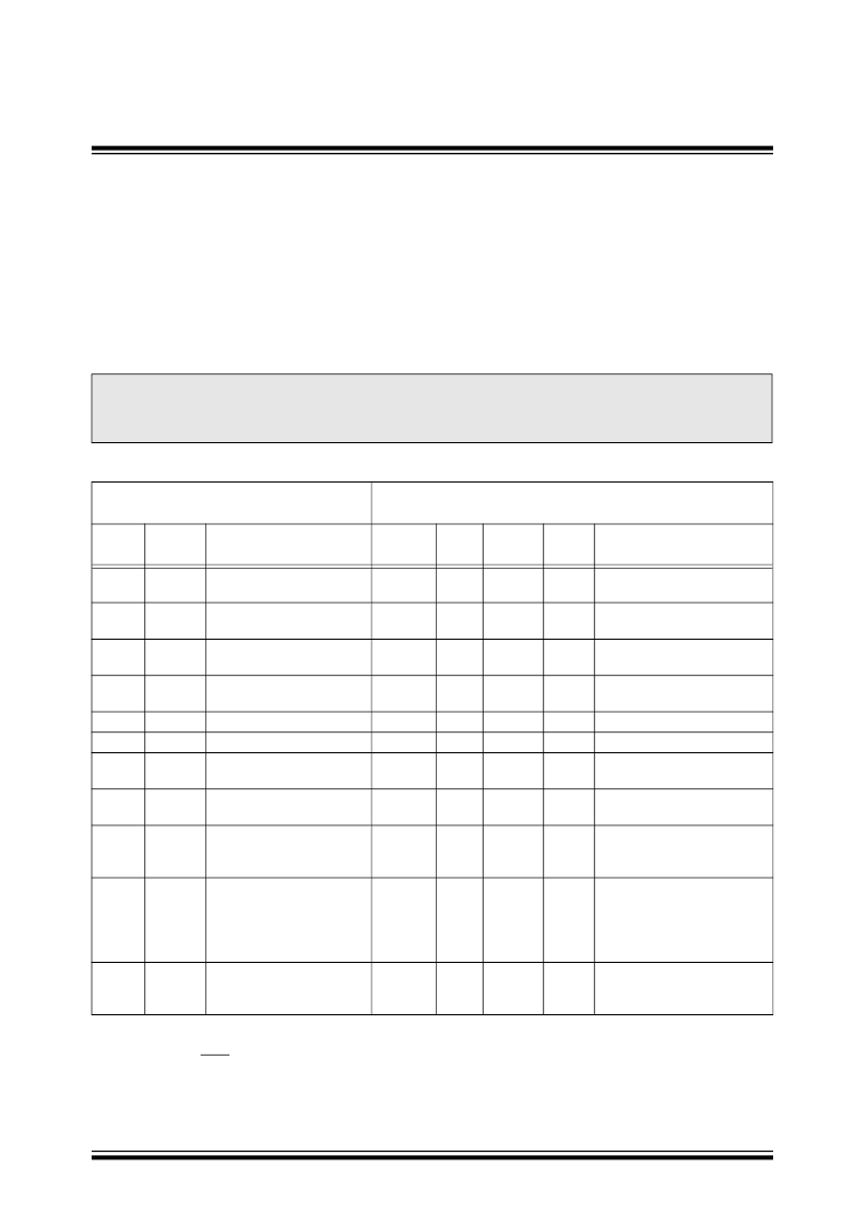
TABLE 1-1:
DC CHARACTERISTICS
NOTICE: Stresses above those listed under “Absolute Maximum Ratings” may cause permanent damage to the
device. This is a stress rating only and functional operation of the device at those or any other conditions above those
indicated in the operational listings of this specification is not implied. Exposure to maximum rating conditions for
extended periods may affect device reliability.
All parameters apply over the specified
ranges unless otherwise noted.
Industrial (I):
Automotive (E): T
A
= -40°C to +125°C, V
CC
= +2.5V to 5.5V
T
A
= -40°C to +85°C, V
CC
= +1.8V to 5.5V
Param.
No.
Symbol
Parameter
Min
Typ
Max
Units
Conditions
D1
V
IH
1
V
IH
2
V
IL
1
V
IL
2
V
OL
1
V
OL
2
V
OH
1
V
OH
2
I
LI
I
LO
C
IN
,
C
OUT
I
CC
write Write current
High-level input voltage
2.0
0.7 V
CC
-0.3
-0.3
—
—
2.4
V
CC
- 0.2
—
—
—
—
—
—
—
—
—
—
—
—
—
—
V
CC
+1
V
CC
+1
0.8
0.2 V
CC
0.4
0.2
—
—
±1
±1
7
V
V
V
V
V
V
V
V
μ
A
μ
A
pF
V
CC
≥
2.7V
V
CC
< 2.7V
V
CC
≥
2.7V
V
CC
< 2.7V
I
OL
= 2.1 mA, V
CC
= 4.5V
I
OL
= 100
μ
A, V
CC
= 2.5V
I
OH
= -400
μ
A, V
CC
= 4.5V
I
OH
= -100
μ
A, V
CC
= 2.5V
V
IN
= V
SS
or V
CC
V
OUT
= V
SS
or V
CC
V
IN
/V
OUT
= 0V
(Note 1)
T
A
= 25°C, F
CLK
= 1 MHz
F
CLK
= 3 MHz, V
CC
= 5.5V
F
CLK
= 2 MHz, V
CC
= 2.5V
F
CLK
= 3 MHz, V
CC
= 5.5V
F
CLK
= 2 MHz, V
CC
= 3.0V
F
CLK
= 2 MHz, V
CC
= 2.5V
I – Temp
E – Temp
CLK = CS = 0V
ORG = DI = PE = V
SS
or V
CC
(Note 2) (Note 3)
(Note 1)
93AA76A/B/C, 93LC76A/B/C
93C76A/B/C
D2
Low-level input voltage
D3
Low-level output voltage
D4
High-level output voltage
D5
D6
D7
Input leakage current
Output leakage current
Pin capacitance (all inputs/
outputs)
D8
—
—
—
—
—
—
—
—
500
—
—
100
—
—
3
—
1
500
—
1
5
mA
μ
A
mA
μ
A
μ
A
μ
A
μ
A
D9
I
CC
read
Read current
D10
I
CCS
Standby current
D11
V
POR
V
CC
voltage detect
—
—
1.5
3.8
—
—
V
V
Note 1:
This parameter is periodically sampled and not 100% tested.
ORG and PE pins not available on ‘A’ or ‘B’ versions.
Ready/Busy status must be cleared from DO, see
Section 3.4 “Data Out (DO)”
.
2:
3:
相關(guān)PDF資料 |
PDF描述 |
|---|---|
| 93AA76B | 8K Microwire Compatible Serial EEPROM |
| 93AA76 | Serial EEPROM |
| 93AA76P | Microwire Serial EEPROM |
| 93AA76SN | Microwire Serial EEPROM |
| 93AA76TSN | Microwire Serial EEPROM |
相關(guān)代理商/技術(shù)參數(shù) |
參數(shù)描述 |
|---|---|
| 93AA76C/S15K | 制造商:Microchip Technology Inc 功能描述:8K, 512 X 16 OR 1024 X 8 SERIA - Gel-pak, waffle pack, wafer, diced wafer on film |
| 93AA76C/W15K | 制造商:Microchip Technology Inc 功能描述:8K, 512 X 16 OR 1024 X 8 SERIA - Gel-pak, waffle pack, wafer, diced wafer on film |
| 93AA76C/WF15K | 制造商:Microchip Technology Inc 功能描述:8K, 512 X 16 OR 1024 X 8 SERIA - Gel-pak, waffle pack, wafer, diced wafer on film |
| 93AA76C-I/MS | 功能描述:電可擦除可編程只讀存儲(chǔ)器 516x8-1024x8 - 1.8V RoHS:否 制造商:Atmel 存儲(chǔ)容量:2 Kbit 組織:256 B x 8 數(shù)據(jù)保留:100 yr 最大時(shí)鐘頻率:1000 KHz 最大工作電流:6 uA 工作電源電壓:1.7 V to 5.5 V 最大工作溫度:+ 85 C 安裝風(fēng)格:SMD/SMT 封裝 / 箱體:SOIC-8 |
| 93AA76C-I/MSG | 功能描述:電可擦除可編程只讀存儲(chǔ)器 516x8-1024x8 - 1.8V Lead Free Package RoHS:否 制造商:Atmel 存儲(chǔ)容量:2 Kbit 組織:256 B x 8 數(shù)據(jù)保留:100 yr 最大時(shí)鐘頻率:1000 KHz 最大工作電流:6 uA 工作電源電壓:1.7 V to 5.5 V 最大工作溫度:+ 85 C 安裝風(fēng)格:SMD/SMT 封裝 / 箱體:SOIC-8 |
發(fā)布緊急采購(gòu),3分鐘左右您將得到回復(fù)。