- 您現(xiàn)在的位置:買賣IC網(wǎng) > PDF目錄360636 > 96L02DMQB (NATIONAL SEMICONDUCTOR CORP) Dual Retriggerable Resettable Monostable Multivibrator PDF資料下載
參數(shù)資料
| 型號: | 96L02DMQB |
| 廠商: | NATIONAL SEMICONDUCTOR CORP |
| 元件分類: | 諧振器 |
| 英文描述: | Dual Retriggerable Resettable Monostable Multivibrator |
| 中文描述: | 96L SERIES, DUAL MONOSTABLE MULTIVIBRATOR, CDIP16 |
| 封裝: | CERAMIC, DIP-16 |
| 文件頁數(shù): | 3/6頁 |
| 文件大?。?/td> | 144K |
| 代理商: | 96L02DMQB |
Switching Characteristics
V
CC
e a
5.0V, T
A
e a
25
§
C
Symbol
Parameter
Conditions
96L02 (Mil)
DM96L02 (Com)
Units
Min
Max
Min
Max
t
PLH
Propagation Delay I0 to Q,
I1 to Q
V
CC
e
5.0V, R
X
e
20 k
X
C
X
e
0, C
L
e
15 pF
75
80
ns
t
PHL
Propagation Delay I0 to Q,
I1 to Q
V
CC
e
5.0V, R
X
e
20 k
X
C
X
e
0, C
L
e
15 pF
62
65
ns
t
PLH
t
PHL
Propagation Delay CD to Q,
CD to Q
V
CC
e
5.0V, R
X
e
39 k
X
C
X
e
1000 pF
100
ns
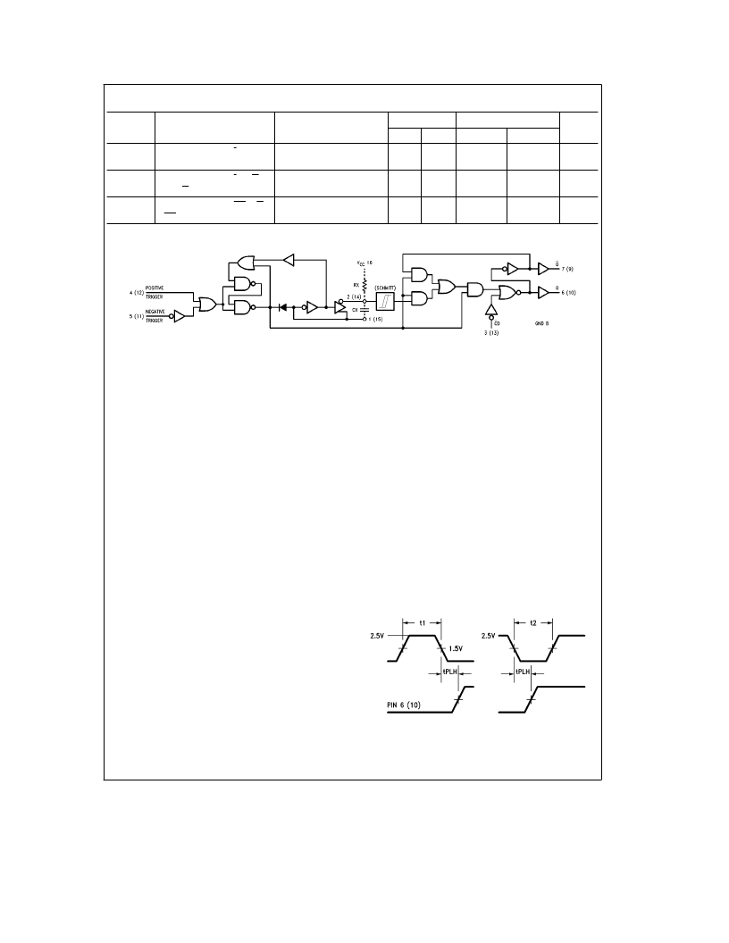
Functional Block Diagram
TL/F/10203–3
Operation Notes
1. TRIGGERINGDcan be accomplished by a positive-going
transition on pin 4 (12) or a negative-going transition on
pin 5 (11). Triggering begins as a signal crosses the input
V
IL
:V
IH
threshold region; this activates an internal latch
whose unbalanced cross-coupling causes it to assume a
preferred state. As the latch output goes LOW it disables
the gates leading to the Q output and, through an invert-
er, turns on the capacitor discharge transistor. The invert-
ed signal is also fed back to the latch input to change its
state and effectively end the triggering action; thus the
latch and its associated feed-back perform the function of
a differentiator.
The emitters of the latch transistors return to ground
through an enabling transistor which must be turned off
between successive triggers in order for the latch to pro-
ceed through the proper sequence when triggering is de-
sired. Pin 5 (11) must be HIGH in order to trigger at pin 4
(12); conversely, pin 4 (12) must be LOW in order to trig-
ger at pin 5 (11).
2. RETRIGGERINGDIn a normal cycle, triggering initiates a
rapid discharge of the external timing capacitor, followed
by a ramp voltage run-up at pin 2 (14). The delay will time
out when the ramp voltage reaches the upper trigger
point of a Schmitt circuit, causing the outputs to revert to
the quiescent state. If another trigger occurs before the
ramp voltage reaches the Schmitt threshold, the capaci-
tor will be discharged and the ramp will start again without
having disturbed the output. The delay period can there-
fore be extended for an arbitrary length of time by insur-
ing that the interval between triggers is less than the de-
lay time, as determined by the external capacitor and re-
sistor.
3. NON-RETRIGGERABLE OPERATIONDRetriggering can
be inhibited logically, by connecting pin 6 (10) back to pin
4 (12) or by connecting pin 7 (9) back to pin 5 (11). Either
hook-up has the effect of keeping the latch-enabling tran-
sistor turned on during the delay period, which prevents
the input latch from cycling as discussed above in the
section on triggering.
4. OUTPUT PULSE WIDTHDAn external resistor R
X
and an
external capacitor C
X
are required, as shown in the func-
tional block diagram. To minimize stray capacitance and
noise pickup, R
X
and C
X
should be located as close as
possible to the circuit. In applications which require re-
mote trimming of the pulse width, as with a variable resis-
tor, R
X
should consist of a fixed resistor in series with the
variable resistor; the fixed resistor should be located as
close as possible to the circuit. The output pulse width t
w
is defined as follows, where R
X
is in k
X
, C
X
is in pF and
t
w
is in ns.
t
w
e
0.33 R
X
C
X
(1
a
3/R
X
) for C
X
t
10
3
pF
16 k
X
s
R
X
s
220 k
X
for 0
§
C to
a
75
§
C
20 k
X
s
R
X
s
100 k
X
for
b
55
§
C to
a
125
§
C
C
X
may vary from 0 to any value. For pulse widths with C
X
less than 10
3
pF see Figure a.
5. SETUP AND RELEASE TIMESDThe setup times listed
below are necessary to allow the latch-enabling transistor
to turn off and the node voltages within the input latch to
stabilize, thus insuring proper cycling of the latch when
the next trigger occurs. The indicated release times
(equivalent to trigger duration) allow time for the input
latch to cycle and its signal to propagate.
Input to Pin 5 (11)
Pin 4 (12)
e
L
Pin 3 (13)
e
H
TL/F/10203–4
3
相關PDF資料 |
PDF描述 |
|---|---|
| 96L02FMQB | Dual Retriggerable Resettable Monostable Multivibrator |
| 96LS02DMQB | Monostable Multivibrator |
| 96LS02FMQB | Monostable Multivibrator |
| 96LS02 | Dual Retriggerable Resettable Monostable Multivibrator |
| 96SCRP11 | SOLDER CREAM AGS 88.5 250G |
相關代理商/技術參數(shù) |
參數(shù)描述 |
|---|---|
| 96L02FM/B | 制造商:Rochester Electronics LLC 功能描述: |
| 96L02FMQB | 制造商:NSC 制造商全稱:National Semiconductor 功能描述:Dual Retriggerable Resettable Monostable Multivibrator |
| 96L02PC | 制造商:Rochester Electronics LLC 功能描述:- Bulk |
| 96-LA | 制造商:Edwards Signaling & Security Systems 功能描述:LENS Amber |
| 96LC1-20-1-B | 制造商:POLAMCO 功能描述:STRAIN RELIEF ADAPTOR, SIZE 20 |
發(fā)布緊急采購,3分鐘左右您將得到回復。