- 您現(xiàn)在的位置:買賣IC網(wǎng) > PDF目錄67355 > A1392SEHLT-T MAGNETIC FIELD SENSOR-HALL EFFECT, 3.1V, RECTANGULAR, SURFACE MOUNT PDF資料下載
參數(shù)資料
| 型號(hào): | A1392SEHLT-T |
| 元件分類: | 磁阻傳感器 |
| 英文描述: | MAGNETIC FIELD SENSOR-HALL EFFECT, 3.1V, RECTANGULAR, SURFACE MOUNT |
| 封裝: | 2 X 3 MM, 0.75 MM HEIGHT, LEAD FREE, DFN-6 |
| 文件頁(yè)數(shù): | 7/15頁(yè) |
| 文件大小: | 480K |
| 代理商: | A1392SEHLT-T |
第1頁(yè)第2頁(yè)第3頁(yè)第4頁(yè)第5頁(yè)第6頁(yè)當(dāng)前第7頁(yè)第8頁(yè)第9頁(yè)第10頁(yè)第11頁(yè)第12頁(yè)第13頁(yè)第14頁(yè)第15頁(yè)
Micro Power 3 V Linear Hall Effect Sensor ICs
with Tri-State Output and User Selectable Sleep Mode
A1391, A1392,
A1393, and A1395
15
Allegro MicroSystems, Inc.
115 Northeast Cutoff, Box 15036
Worcester, Massachusetts 01615-0036 (508) 853-5000
www.allegromicro.com
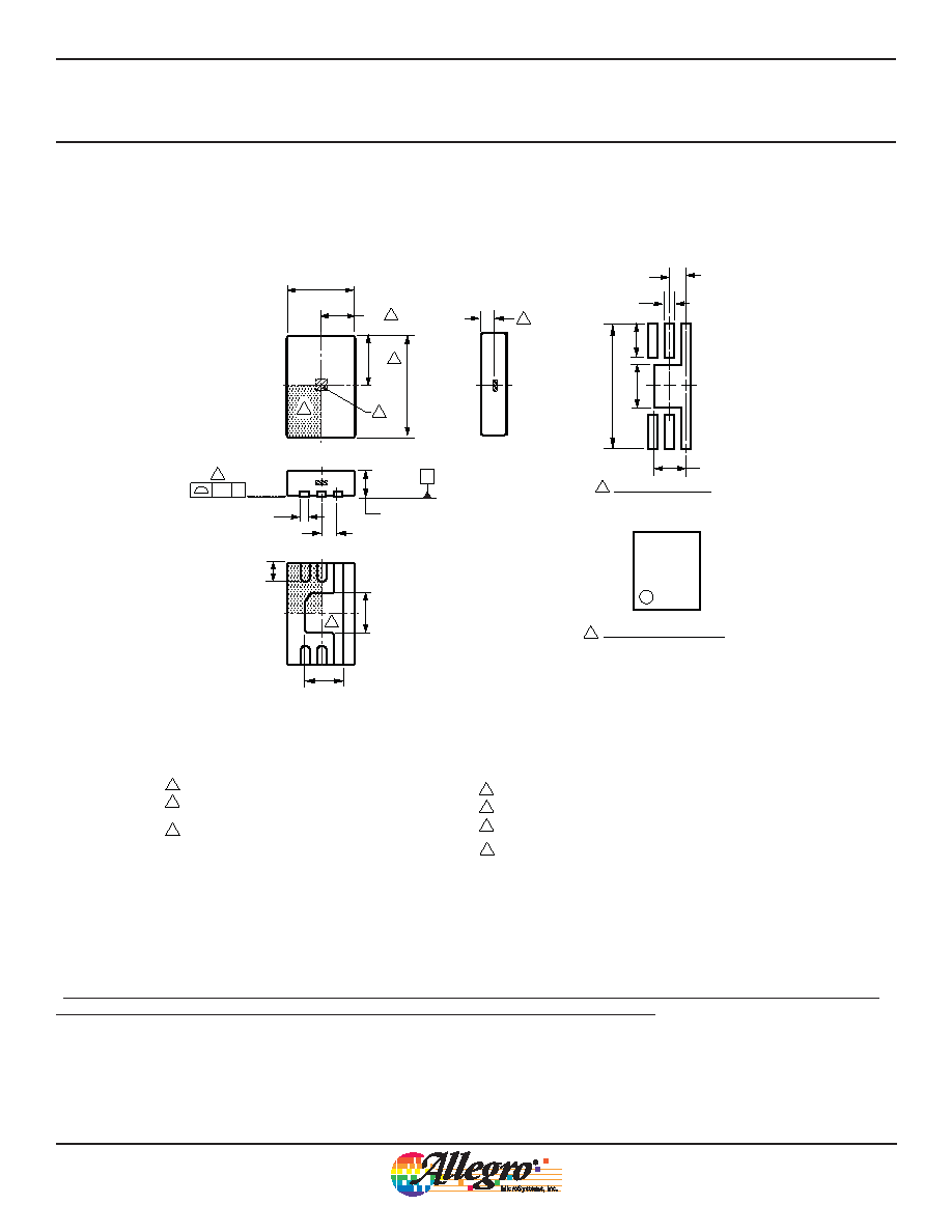
Package EH, 6-pin MLP/DFN
For the latest version of this document, visit our website:
www.allegromicro.com
Copyright 2005-2010, Allegro MicroSystems, Inc.
Allegro MicroSystems, Inc. reserves the right to make, from time to time, such departures from the detail specifications as may be required to per-
mit improvements in the performance, reliability, or manufacturability of its products. Before placing an order, the user is cautioned to verify that the
information being relied upon is current.
Allegro’s products are not to be used in life support devices or systems, if a failure of an Allegro product can reasonably be expected to cause the
failure of that life support device or system, or to affect the safety or effectiveness of that device or system.
The information included herein is believed to be accurate and reliable. However, Allegro MicroSystems, Inc. assumes no responsibility for its use;
nor for any infringement of patents or other rights of third parties which may result from its use.
C
0.08
7X
C
SEATING
PLANE
6
2
1
A
Terminal #1 mark area
B
Exposed thermal pad (reference only, terminal #1
identifier appearance at supplier discretion)
For Reference Only, not for tooling use (reference DWG-2861;
reference JEDEC MO-229WCED, Type 1)
Dimensions in millimeters
Exact case and lead configuration at supplier discretion within limits shown
C
Reference land pattern layout;
All pads a minimum of 0.20 mm from all adjacent pads; adjust as
necessary to meet application process requirements and PCB layout
tolerances; when mounting on a multilayer PCB, thermal vias at the
exposed thermal pad land can improve thermal dissipation (reference
EIA/JEDEC Standard JESD51-5)
Hall Element (not to scale); U.S. customary dimensions controlling
Branding scale and appearance at supplier discretion
E
1
6
B
2
F
E
F
Active Area Depth, 0.32 mm NOM
1.00
3.70 1.25
0.50
0.95
0.30
1
6
G
PCB Layout Reference View
C
2.00 ±0.15
1.00
1.50
3.00 ±0.15
0.75 ±0.05
1.224 ±0.050
1.042
+0.100
–0.150
0.25 ±0.05
0.5 BSC
0.55 ±0.10
D
Coplanarity includes exposed thermal pad and terminals
Standard Branding Reference View
Y = Last two digits of year of manufacture
W = Week of manufacture
L = Lot number
N = Last two digits of device part number
YWW
LLL
NN
1
相關(guān)PDF資料 |
PDF描述 |
|---|---|
| A1393SEHLT-T | MAGNETIC FIELD SENSOR-HALL EFFECT, 3.1V, RECTANGULAR, SURFACE MOUNT |
| A1642LKTN-I2-T | MAGNETIC FIELD SENSOR-HALL EFFECT, 3-100mT, RECTANGULAR, THROUGH HOLE MOUNT |
| A3421LKA-TL | MAGNETIC FIELD SENSOR-HALL EFFECT, -28-28mT, 0.21-0.50V, RECTANGULAR, THROUGH HOLE MOUNT |
| A3422EKA-TL | MAGNETIC FIELD SENSOR-HALL EFFECT, -7.5-7.5mT, 0.21-0.50V, RECTANGULAR, THROUGH HOLE MOUNT |
| A3515EUA | MAGNETIC FIELD SENSOR-HALL EFFECT, 1mT, 0.2-4.7V, RECTANGULAR, THROUGH HOLE MOUNT |
相關(guān)代理商/技術(shù)參數(shù) |
參數(shù)描述 |
|---|---|
| A1392SEHLT-T | 制造商:Allegro MicroSystems 功能描述:Hall Effect IC |
| A1392SEHLT-TCUT | 制造商:Allegro MicroSystems LLC 功能描述: |
| A1392SEHLX-T | 制造商:Allegro MicroSystems 功能描述:LOW POWER LINEAR HALL-EFFECT S 制造商:ALLEGRO MICROSYSTEMS, LLC 功能描述:IC HALL EFFECT SENSOR 6-MLP |
| A1393 | 制造商:Hakko 功能描述:A1393 Nozzle |
| A1393/P | 制造商:HAKKO Corporation 功能描述: |
發(fā)布緊急采購(gòu),3分鐘左右您將得到回復(fù)。