- 您現(xiàn)在的位置:買賣IC網(wǎng) > PDF目錄294787 > A32400DX-1PQ240C FPGA, 2526 CLBS, 40000 GATES, PQFP240 PDF資料下載
參數(shù)資料
| 型號(hào): | A32400DX-1PQ240C |
| 元件分類: | FPGA |
| 英文描述: | FPGA, 2526 CLBS, 40000 GATES, PQFP240 |
| 封裝: | PLASTIC, QFP-240 |
| 文件頁(yè)數(shù): | 20/22頁(yè) |
| 文件大小: | 217K |
| 代理商: | A32400DX-1PQ240C |
第1頁(yè)第2頁(yè)第3頁(yè)第4頁(yè)第5頁(yè)第6頁(yè)第7頁(yè)第8頁(yè)第9頁(yè)第10頁(yè)第11頁(yè)第12頁(yè)第13頁(yè)第14頁(yè)第15頁(yè)第16頁(yè)第17頁(yè)第18頁(yè)第19頁(yè)當(dāng)前第20頁(yè)第21頁(yè)第22頁(yè)

7
3200DX Field Programmable Gate Arrays – The System Logic Integrator Family
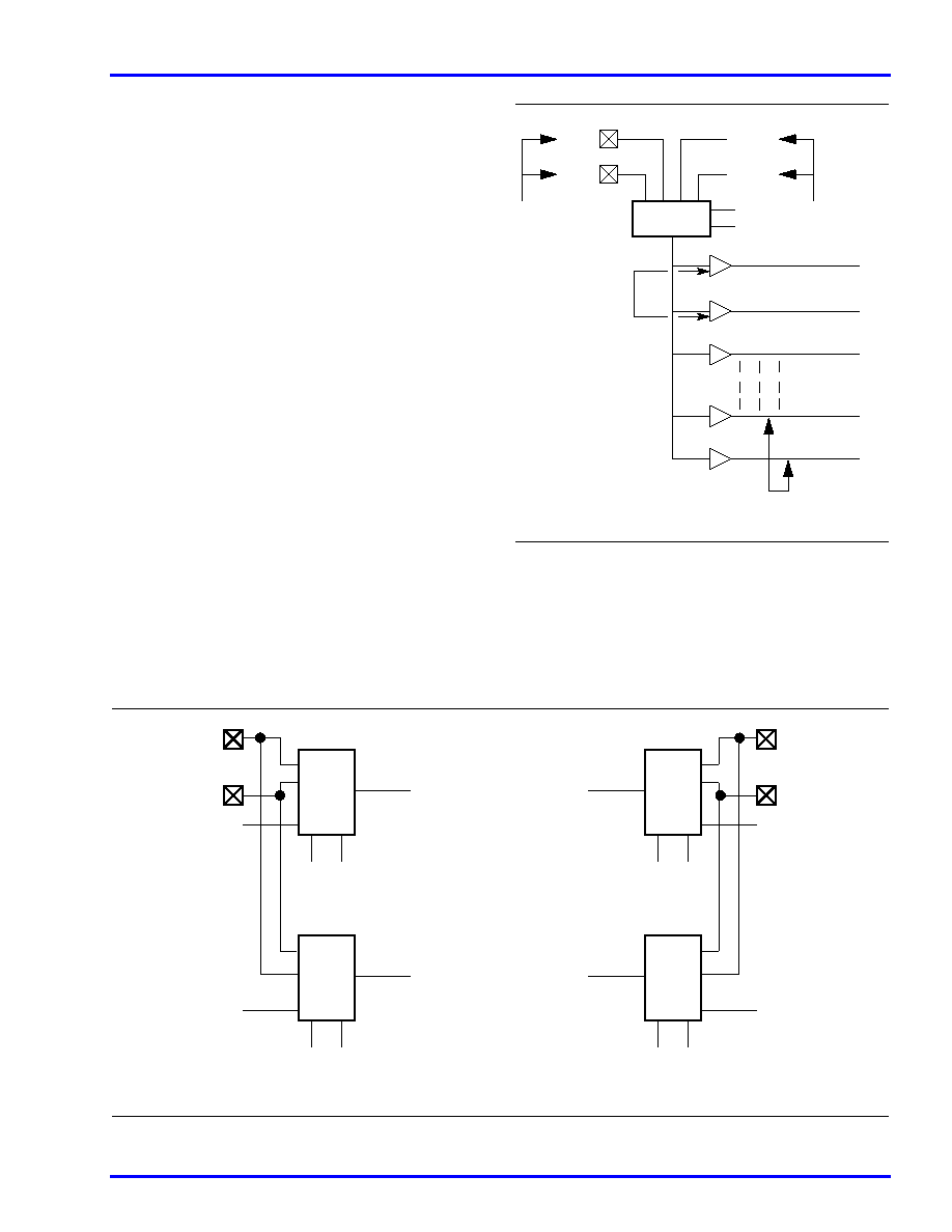
Clock Networks
Two low-skew, high fanout clock distribution networks are
provided in each 3200DX device. These networks are
referred to as CLK0 and CLK1. Each network has a clock
module (CLKMOD) that selects the source of the clock
signal and may be driven as follows:
1.
Externally from the CLKA pad
2.
Externally from the CLKB pad
3.
Internally from the CLKINA input
4.
Internally from the CLKINB input
The clock modules are located in the top row of I/O modules.
Clock drivers and a dedicated horizontal clock track are
located in each horizontal routing channel.
The user controls the clock module by selecting one of two
clock macros from the macro library. The macro CLKBUF is
used to connect one of the two external clock pins to a clock
network, and the macro CLKINT is used to connect an
internally generated clock signal to a clock network. Since
both clock networks are identical, the user does not care
whether CLK0 or CLK1 is being used. The clock input pads
may also be used as normal I/Os, bypassing the clock
networks (see Figure 7).
The 3200DX devices which contain SRAM modules (all
except A3265DX and A32140DX) have four additional
register control resources, called Quadrant Clock Networks
(Figure 8). Each quadrant clock provides a local, high-fanout
resource to the contiguous logic modules within its quadrant
of the device. Quadrant clock signals can originate from
specific I/O pins or from the internal array and can be used as
a secondary register clock, register clear, or output enable.
Test Circuitry
The 3200DX provides two modes of device and/or
board-level testing; JTAG 1149.1 Boundary Scan Testing
and Actel’s Actionprobe test facility. Once a 3200DX
device has been programmed, the Actionprobe test facility
Figure 7 Clock Networks
CLKB
CLKA
FROM
PADS
CLOCK
DRIVERS
CLKMOD
CLKINB
CLKINA
S0
S1
INTERNAL
SIGNAL
CLKO(17)
CLKO(16)
CLKO(15)
CLKO(2)
CLKO(1)
CLOCK TRACKS
Figure 8 Quadrant Clock Network
Quad
Clock
Module
QCLKA
QCLKB
*QCLK1IN
S0 S1
QCLK1
Quad
Clock
Module
*QCLK2IN
S0 S1
QCLK2
Quad
Clock
Module
QCLKC
QCLKD
*QCLK3IN
S0
S1
QCLK3
Quad
Clock
Module
*QCLK4IN
S0
S1
QCLK4
*QCLK1IN, QCLK2IN, QCLK3IN, and QCKL4IN are internally generated signals.
相關(guān)PDF資料 |
PDF描述 |
|---|---|
| A32400DX-1PQ240I | FPGA, 2526 CLBS, 40000 GATES, PQFP240 |
| A32400DX-2BG313C | FPGA, 2526 CLBS, 40000 GATES, PBGA313 |
| A32400DX-2BG313I | FPGA, 2526 CLBS, 40000 GATES, PBGA313 |
| A32400DX-2PQ240C | FPGA, 2526 CLBS, 40000 GATES, PQFP240 |
| A32400DX-2PQ240I | FPGA, 2526 CLBS, 40000 GATES, PQFP240 |
相關(guān)代理商/技術(shù)參數(shù) |
參數(shù)描述 |
|---|---|
| A32400DX-1RQ240C | 制造商:未知廠家 制造商全稱:未知廠家 功能描述:Field Programmable Gate Array (FPGA) |
| A32400DX-1RQ240I | 制造商:未知廠家 制造商全稱:未知廠家 功能描述:Field Programmable Gate Array (FPGA) |
| A32400DX-2RQ240C | 制造商:未知廠家 制造商全稱:未知廠家 功能描述:Field Programmable Gate Array (FPGA) |
| A32400DX-2RQ240I | 制造商:未知廠家 制造商全稱:未知廠家 功能描述:Field Programmable Gate Array (FPGA) |
| A32400DX-3RQ240C | 制造商:未知廠家 制造商全稱:未知廠家 功能描述:Field Programmable Gate Array (FPGA) |
發(fā)布緊急采購(gòu),3分鐘左右您將得到回復(fù)。