- 您現(xiàn)在的位置:買賣IC網(wǎng) > PDF目錄298742 > A42MX02-2TQ100B (Electronic Theatre Controls, Inc.) 40MX and 42MX FPGA Families PDF資料下載
參數(shù)資料
| 型號: | A42MX02-2TQ100B |
| 廠商: | Electronic Theatre Controls, Inc. |
| 英文描述: | 40MX and 42MX FPGA Families |
| 中文描述: | 40MX和42MX FPGA系列 |
| 文件頁數(shù): | 17/53頁 |
| 文件大?。?/td> | 854K |
| 代理商: | A42MX02-2TQ100B |
第1頁第2頁第3頁第4頁第5頁第6頁第7頁第8頁第9頁第10頁第11頁第12頁第13頁第14頁第15頁第16頁當前第17頁第18頁第19頁第20頁第21頁第22頁第23頁第24頁第25頁第26頁第27頁第28頁第29頁第30頁第31頁第32頁第33頁第34頁第35頁第36頁第37頁第38頁第39頁第40頁第41頁第42頁第43頁第44頁第45頁第46頁第47頁第48頁第49頁第50頁第51頁第52頁第53頁
40MX and 42MX FPGA Families
1- 18
v6.0
Mixed 5.0V/3.3V Operating Conditions (for 42MX Devices Only)
Mixed 5.0V/3.3V Electrical Specifications
Table 14
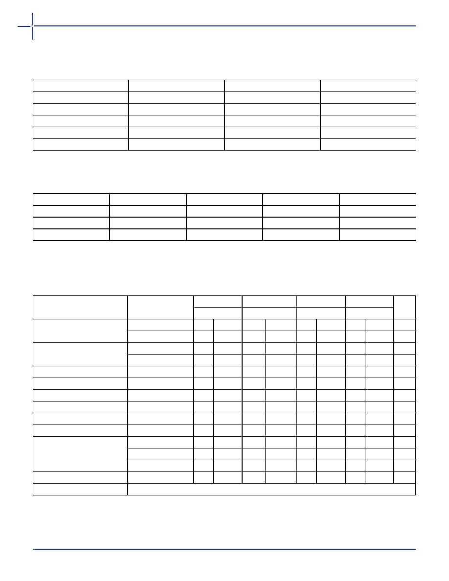
Absolute Maximum Ratings*
Symbol
Parameter
Limits
Units
VCCI
DC Supply Voltage for I/Os
–0.5 to +7.0
V
VCCA
DC Supply Voltage for Array
–0.5 to +7.0
V
VI
Input Voltage
–0.5 to VCCI+0.5
V
VO
Output Voltage
–0.5 to VCCI+0.5
V
tSTG
Storage Temperature
–65 to +150
°C
Note: *Stresses beyond those listed under "Absolute Maximum Ratings" may cause permanent damage to the device. Exposure to
absolute maximum rated conditions for extended periods may affect device reliability. Devices should not be operated outside the
Recommended Operating Conditions.
Table 15
Recommended Operating Conditions
Parameter
Commercial
Industrial
Military
Units
Temperature Range*
0 to +70
-40 to +85
–55 to +125
°C
VCCA
4.75 to 5.25
4.5 to 5.5
V
VCCI
3.14 to 3.47
3.0 to 3.6
V
Note: *Ambient temperature (TA) is used for commercial and industrial grades; case temperature (TC) is used for military grades.
Table 16
Mixed 5.0V/3.3V Electrical Specifications
Symbol
Parameter
Commercial
Commercial '-F
'Industrial
Military
Units
Min.
Max.
Min.
Max.
Min.
Max.
Min.
Max.
VOH
1
IOH = –10mA
2.4
V
IOH = –4mA
3.7
V
VOL
1
IOL = 10mA
0.5
V
IOL = 6mA
0.4
V
VIL
–0.3
0.8
–0.3
0.8
–0.3
0.8
–0.3
0.8
V
VIH
2.0
VCCI+0.3
2.0
VCCI+0.3
2.0
VCCI+0.3 2.0 VCCI+0.3
V
IL
VIN = 0.5V
–10
A
IH
VIN = 2.7V
–10
A
Input Transition Time, TR and TF
500
ns
CIO I/O Capacitance
10
pF
Standby Current, ICC
2
A42MX09
5
25
mA
A42MX16
6
25
mA
A42MX24, A42MX36
20
25
mA
Low-Power Mode Standby Current
0.5
ICC - 5.0
mA
IIO I/O source sink current
Can be derived from the IBIS model (http://www.actel.com/techdocs/models/ibis.html)
Notes:
1. Only one output tested at a time. VCCI = min.
2. All outputs unloaded. All inputs = VCCI or GND.
相關(guān)PDF資料 |
PDF描述 |
|---|---|
| A42MX02-2TQ100ES | 40MX and 42MX FPGA Families |
| A42MX02-2VQ100 | 40MX and 42MX FPGA Families |
| A42MX02-2VQ100A | 40MX and 42MX FPGA Families |
| A42MX02-2VQ100B | 40MX and 42MX FPGA Families |
| A42MX02-2VQ100ES | 40MX and 42MX FPGA Families |
相關(guān)代理商/技術(shù)參數(shù) |
參數(shù)描述 |
|---|---|
| A42MX02-2TQ100ES | 制造商:未知廠家 制造商全稱:未知廠家 功能描述:40MX and 42MX FPGA Families |
| A42MX02-2TQ100I | 制造商:未知廠家 制造商全稱:未知廠家 功能描述:40MX and 42MX FPGA Families |
| A42MX02-2TQ100M | 制造商:未知廠家 制造商全稱:未知廠家 功能描述:40MX and 42MX FPGA Families |
| A42MX02-2VQ100 | 制造商:未知廠家 制造商全稱:未知廠家 功能描述:40MX and 42MX FPGA Families |
| A42MX02-2VQ100A | 制造商:未知廠家 制造商全稱:未知廠家 功能描述:40MX and 42MX FPGA Families |
發(fā)布緊急采購,3分鐘左右您將得到回復(fù)。