- 您現(xiàn)在的位置:買(mǎi)賣(mài)IC網(wǎng) > PDF目錄362023 > A42MX24-2TQ176M Field Programmable Gate Array (FPGA) PDF資料下載
參數(shù)資料
| 型號(hào): | A42MX24-2TQ176M |
| 英文描述: | Field Programmable Gate Array (FPGA) |
| 中文描述: | 現(xiàn)場(chǎng)可編程門(mén)陣列(FPGA) |
| 文件頁(yè)數(shù): | 49/116頁(yè) |
| 文件大?。?/td> | 3110K |
| 代理商: | A42MX24-2TQ176M |
第1頁(yè)第2頁(yè)第3頁(yè)第4頁(yè)第5頁(yè)第6頁(yè)第7頁(yè)第8頁(yè)第9頁(yè)第10頁(yè)第11頁(yè)第12頁(yè)第13頁(yè)第14頁(yè)第15頁(yè)第16頁(yè)第17頁(yè)第18頁(yè)第19頁(yè)第20頁(yè)第21頁(yè)第22頁(yè)第23頁(yè)第24頁(yè)第25頁(yè)第26頁(yè)第27頁(yè)第28頁(yè)第29頁(yè)第30頁(yè)第31頁(yè)第32頁(yè)第33頁(yè)第34頁(yè)第35頁(yè)第36頁(yè)第37頁(yè)第38頁(yè)第39頁(yè)第40頁(yè)第41頁(yè)第42頁(yè)第43頁(yè)第44頁(yè)第45頁(yè)第46頁(yè)第47頁(yè)第48頁(yè)當(dāng)前第49頁(yè)第50頁(yè)第51頁(yè)第52頁(yè)第53頁(yè)第54頁(yè)第55頁(yè)第56頁(yè)第57頁(yè)第58頁(yè)第59頁(yè)第60頁(yè)第61頁(yè)第62頁(yè)第63頁(yè)第64頁(yè)第65頁(yè)第66頁(yè)第67頁(yè)第68頁(yè)第69頁(yè)第70頁(yè)第71頁(yè)第72頁(yè)第73頁(yè)第74頁(yè)第75頁(yè)第76頁(yè)第77頁(yè)第78頁(yè)第79頁(yè)第80頁(yè)第81頁(yè)第82頁(yè)第83頁(yè)第84頁(yè)第85頁(yè)第86頁(yè)第87頁(yè)第88頁(yè)第89頁(yè)第90頁(yè)第91頁(yè)第92頁(yè)第93頁(yè)第94頁(yè)第95頁(yè)第96頁(yè)第97頁(yè)第98頁(yè)第99頁(yè)第100頁(yè)第101頁(yè)第102頁(yè)第103頁(yè)第104頁(yè)第105頁(yè)第106頁(yè)第107頁(yè)第108頁(yè)第109頁(yè)第110頁(yè)第111頁(yè)第112頁(yè)第113頁(yè)第114頁(yè)第115頁(yè)第116頁(yè)
v5.0
49
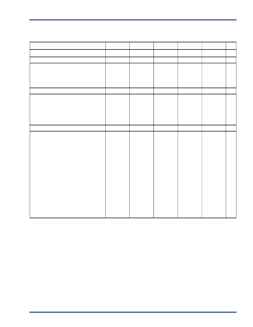
40MX and 42MX FPGA Families
A42MX09 Timing Characteristics (Nominal 3.3V Operation)
(Worst-Case Commercial Conditions, V
CC
= 3.0V, T
J
= 70
°
C)
‘–
3
’
Speed
‘–
2
’
Speed
‘–
1
’
Speed
‘
Std
’
Speed
‘–
F
’
Speed
Parameter Description
Min.
Max.
Min.
Max.
Min.
Max.
Min.
Max.
Min.
Max.
Units
Logic Module Propagation Delays
1
t
PD1
Single Module
1.6
1.8
2.1
2.5
3.5
ns
t
CO
Sequential Clock-to-Q
1.8
2.0
2.3
2.7
3.8
ns
t
GO
Latch G-to-Q
1.7
1.9
2.1
2.5
3.5
ns
t
RS
Logic Module Predicted Routing Delays
2
Flip-Flop (Latch) Reset-to-Q
2.0
2.2
2.5
2.9
4.1
ns
t
RD1
FO=1 Routing Delay
1.0
1.1
1.2
1.4
2.0
ns
t
RD2
FO=2 Routing Delay
1.3
1.4
1.6
1.9
2.7
ns
t
RD3
FO=3 Routing Delay
1.6
1.8
2.0
2.4
3.3
ns
t
RD4
FO=4 Routing Delay
1.9
2.1
2.4
2.9
4.0
ns
t
RD8
Logic Module Sequential Timing
3, 4
FO=8 Routing Delay
3.2
3.6
4.1
4.8
6.7
ns
t
SUD
Flip-Flop (Latch) Data Input Set-Up
0.5
0.5
0.6
0.7
0.9
ns
t
HD
Flip-Flop (Latch) Data Input Hold
0.0
0.0
0.0
0.0
0.0
ns
t
SUENA
Flip-Flop (Latch) Enable Set-Up
0.6
0.6
0.7
0.8
1.2
ns
t
HENA
Flip-Flop (Latch) Enable Hold
0.0
0.0
0.0
0.0
0.0
ns
t
WCLKA
Flip-Flop (Latch) Clock Active Pulse
Width
4.7
5.3
6.0
7.0
9.8
ns
t
WASYN
Flip-Flop (Latch) Asynchronous Pulse
Width
6.2
6.9
7.8
9.2
12.9
ns
t
A
Flip-Flop Clock Input Period
5.0
5.6
6.2
7.1
9.9
ns
t
INH
Input Buffer Latch Hold
0.0
0.0
0.0
0.0
0.0
ns
t
INSU
Input Buffer Latch Set-Up
0.3
0.3
0.3
0.4
0.6
ns
t
OUTH
Output Buffer Latch Hold
0.0
0.0
0.0
0.0
0.0
ns
t
OUTSU
Output Buffer Latch Set-Up
0.3
0.3
0.3
0.4
0.6
ns
f
MAX
Flip-Flop (Latch) Clock
Frequency
161
146
135
117
70
MHz
Notes:
1.
2.
For dual-module macros, use t
PD1
+ t
RD1
+ t
PDn
, t
CO
+ t
RD1
+ t
PDn
, or t
PD1
+ t
RD1
+ t
SUD
, whichever is appropriate.
Routing delays are for typical designs across worst-case operating conditions. These parameters should be used for estimating device
performance. Post-route timing analysis or simulation is required to determine actual performance.
Data applies to macros based on the S-module. Timing parameters for sequential macros constructed from C-modules can be obtained from
the Timer utility.
Set-up and hold timing parameters for the input buffer latch are defined with respect to the PAD and the D input. External setup/hold
timing parameters must account for delay from an external PAD signal to the G inputs. Delay from an external PAD signal to the G input
subtracts (adds) to the internal setup (hold) time.
3.
4.
發(fā)布緊急采購(gòu),3分鐘左右您將得到回復(fù)。