- 您現(xiàn)在的位置:買賣IC網(wǎng) > PDF目錄379533 > A54SX08P-2PQ208I (Electronic Theatre Controls, Inc.) 54SX Family FPGAs PDF資料下載
參數(shù)資料
| 型號(hào): | A54SX08P-2PQ208I |
| 廠商: | Electronic Theatre Controls, Inc. |
| 元件分類: | FPGA |
| 英文描述: | 54SX Family FPGAs |
| 中文描述: | 54SX家庭的FPGA |
| 文件頁數(shù): | 15/57頁 |
| 文件大?。?/td> | 415K |
| 代理商: | A54SX08P-2PQ208I |
第1頁第2頁第3頁第4頁第5頁第6頁第7頁第8頁第9頁第10頁第11頁第12頁第13頁第14頁當(dāng)前第15頁第16頁第17頁第18頁第19頁第20頁第21頁第22頁第23頁第24頁第25頁第26頁第27頁第28頁第29頁第30頁第31頁第32頁第33頁第34頁第35頁第36頁第37頁第38頁第39頁第40頁第41頁第42頁第43頁第44頁第45頁第46頁第47頁第48頁第49頁第50頁第51頁第52頁第53頁第54頁第55頁第56頁第57頁
v3.1
15
5 4 S X F a m ily F P G A s
A 54S X 16P AC S pec ific ations (3.3V PCI Operation)
Symbol
Parameter
Condition
0 < V
OUT
≤
0.3V
CC1
0.3V
CC
≤
V
OUT
< 0.9V
CC1
Min.
Max.
Units
Switching Current High
mA
mA
–12V
CC
I
OH(AC)
0.7V
CC
< V
OUT
< V
CC1, 2
–17.1 + (V
CC
– V
OUT
)
Equation C: on
page 16
–32V
CC
(Test Point)
V
OUT
= 0.7V
CC2
V
CC
> V
OUT
≥
0.6V
CC1
0.6V
CC
> V
OUT
> 0.1V
CC1
0.18V
CC
> V
OUT
> 0
1, 2
V
OUT
= 0.18V
CC2
–3 < V
IN
≤
–1
–3 < V
IN
≤
–1
0.2V
CC
to 0.6V
CC
load
0.6V
CC
to 0.2V
CC
load
mA
mA
mA
mA
Switching Current High
16V
CC
26.7V
OUT
I
OL(AC)
on page 16
38V
CC
(Test Point)
Low Clamp Current
High Clamp Current
Output Rise Slew Rate
3
Output Fall Slew Rate
3
I
CL
I
CH
slew
R
slew
F
Notes:
1.
–25 + (V
IN
+ 1)/0.015
25 + (V
IN
– V
OUT
– 1)/0.015
1
1
mA
mA
V/ns
V/ns
4
4
Refer to the V/I curves in
Figure9
. Switching current characteristics for REQ#and GNT#are permitted to be one half of that specified here;
i.e., half size output drivers may be used on these signals. This specification does not apply to CLK and RST#which are system outputs.
“Switching Current High” specification are not relevant to SERR# INTA# INTB# INTC# and INTD#which are open drain outputs.
Maximum current requirements must be met as drivers pull beyond the last step voltage. Equations defining these maximums (C and D)
are provided with the respective diagrams in
Figure9
. The equation defined maxima should be met by design. In order to facilitate
component testing, a maximum current test point is defined for each side of the output driver.
This parameter is to be interpreted as the cumulative edge rate across the specified range, rather than the instantaneous rate at any point
within the transition range. The specified load (diagram below) is optional; i.e., the designer may elect to meet this parameter with an
unloaded output per the latest revision of the PCI Local Bus Specification. However, adherence to both maximum and minimum
parameters is required (the maximum is no longer simply a guideline). Rise slew rate does not apply to open drain outputs.
2.
3.
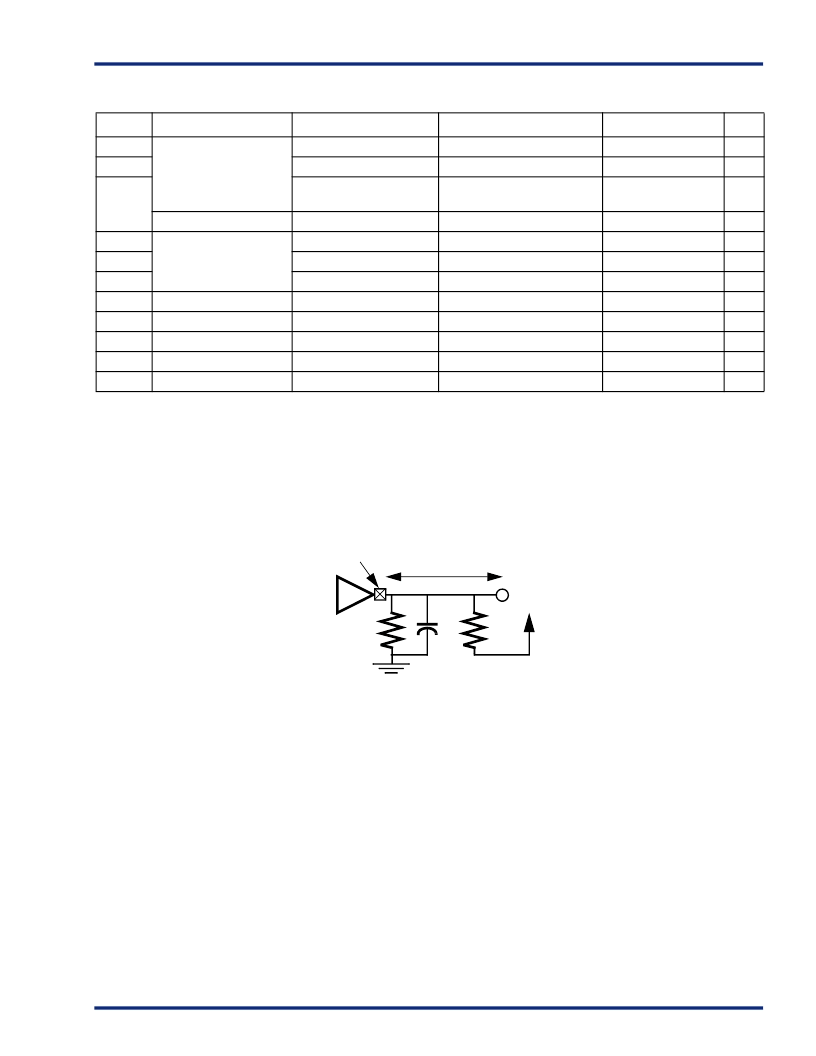
output
buffer
1/2 in. max.
V
CC
1k
10 pF
1k
pin
相關(guān)PDF資料 |
PDF描述 |
|---|---|
| A54SX08P-2PQ208M | 54SX Family FPGAs |
| A54SX08P-2PQ208PP | 54SX Family FPGAs |
| A54SX08P-2TQ208 | 54SX Family FPGAs |
| A54SX08P-2TQ208I | 54SX Family FPGAs |
| A54SX08P-2TQ208PP | 54SX Family FPGAs |
相關(guān)代理商/技術(shù)參數(shù) |
參數(shù)描述 |
|---|---|
| A54SX08P-2PQ208M | 制造商:未知廠家 制造商全稱:未知廠家 功能描述:54SX Family FPGAs |
| A54SX08P-2PQ208PP | 制造商:未知廠家 制造商全稱:未知廠家 功能描述:54SX Family FPGAs |
| A54SX08P-2PQG208 | 制造商:ACTEL 制造商全稱:Actel Corporation 功能描述:SX Family FPGAs |
| A54SX08-P-2PQG208I | 制造商:ACTEL 制造商全稱:Actel Corporation 功能描述:SX Family FPGAs |
| A54SX08P-2PQG208I | 制造商:ACTEL 制造商全稱:Actel Corporation 功能描述:SX Family FPGAs |
發(fā)布緊急采購,3分鐘左右您將得到回復(fù)。