- 您現(xiàn)在的位置:買賣IC網(wǎng) > PDF目錄362029 > A54SX16P-1TQ144M Field Programmable Gate Array (FPGA) PDF資料下載
參數(shù)資料
| 型號(hào): | A54SX16P-1TQ144M |
| 英文描述: | Field Programmable Gate Array (FPGA) |
| 中文描述: | 現(xiàn)場(chǎng)可編程門陣列(FPGA) |
| 文件頁(yè)數(shù): | 20/36頁(yè) |
| 文件大?。?/td> | 833K |
| 代理商: | A54SX16P-1TQ144M |
第1頁(yè)第2頁(yè)第3頁(yè)第4頁(yè)第5頁(yè)第6頁(yè)第7頁(yè)第8頁(yè)第9頁(yè)第10頁(yè)第11頁(yè)第12頁(yè)第13頁(yè)第14頁(yè)第15頁(yè)第16頁(yè)第17頁(yè)第18頁(yè)第19頁(yè)當(dāng)前第20頁(yè)第21頁(yè)第22頁(yè)第23頁(yè)第24頁(yè)第25頁(yè)第26頁(yè)第27頁(yè)第28頁(yè)第29頁(yè)第30頁(yè)第31頁(yè)第32頁(yè)第33頁(yè)第34頁(yè)第35頁(yè)第36頁(yè)
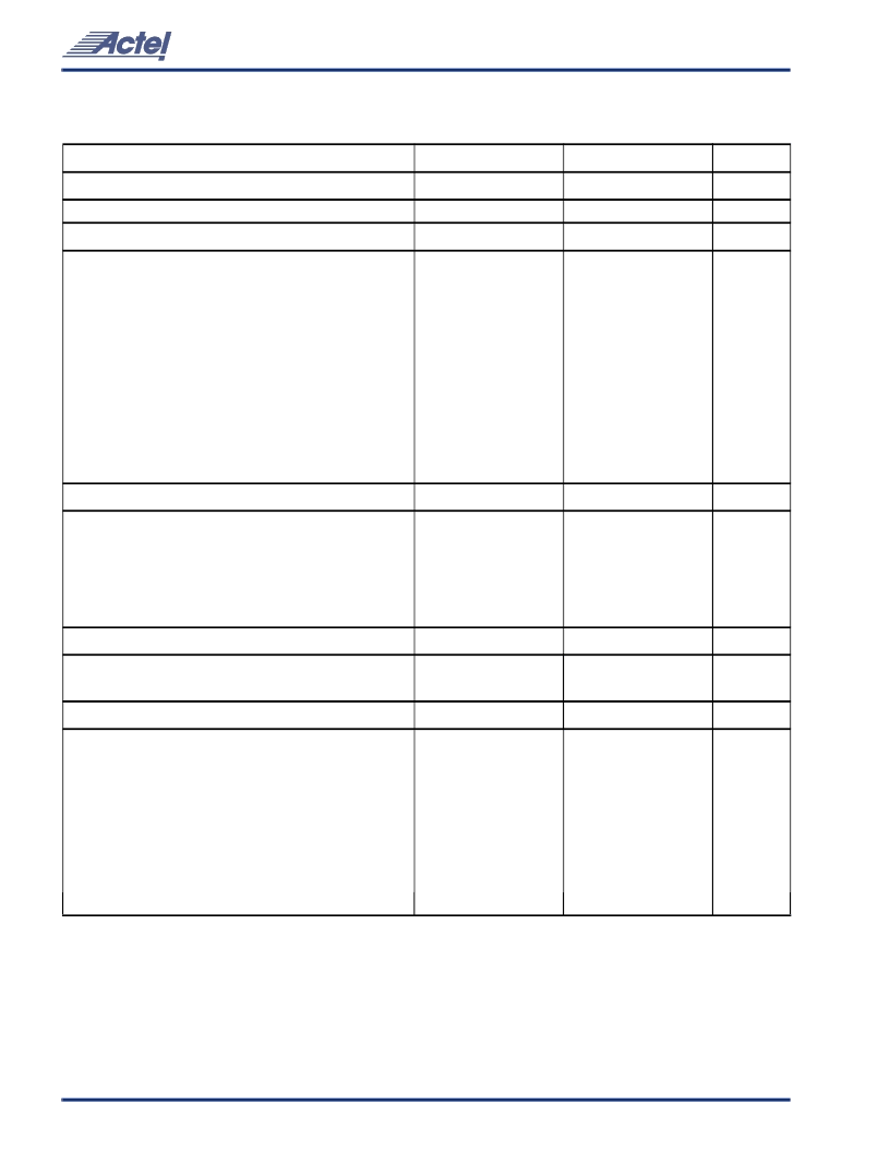
54SX Family FPGAs RadTolerant and HiRel
20
v2.0
RT54SX16 Timing Characteristics
(Worst-Case Military Conditions, V
CCR
= 4.75V, V
CCA,
V
CCI
= 3.0V, T
J
= 125
°
C)
C-Cell Propagation Delays
1
‘–
1
’
Speed
‘
Std
’
Speed
Parameter
Description
Min.
Max.
Min.
Max.
Units
t
PD
Predicted Routing Delays
2
Internal Array Module
1.7
1.8
ns
t
DC
t
FC
t
RD1
t
RD2
t
RD3
t
RD4
t
RD8
t
RD12
t
RD18
t
RD24
FO=1 Routing Delay, Direct Connect
0.2
0.2
ns
FO=1 Routing Delay, Fast Connect
1.1
1.3
ns
FO=1 Routing Delay
1.3
1.5
ns
FO=2 Routing Delay
2.2
2.6
ns
FO=3 Routing Delay
3.1
3.6
ns
FO=4 Routing Delay
4.0
4.7
ns
FO=8 Routing Delay
7.8
9.0
ns
FO=12 Routing Delay
10.1
11.9
ns
FO=18 Routing Delay
17.0
19.8
ns
FO=24 Routing Delay
22.4
26.3
ns
R-Cell Timing
t
RCO
t
CLR
t
SUD
t
HD
t
WASYN
Sequential Clock-to-Q
1.5
2.0
ns
Asynchronous Clear-to-Q
1.5
2.0
ns
Flip-Flop Data Input Set-Up
2.0
2.2
ns
Flip-Flop Data Input Hold
0.0
0.0
ns
Asynchronous Pulse Width
4.4
5.3
ns
I/O Module Input Propagation Delays
t
INYH
t
INYL
Predicted Input Routing Delays
3
Input Data Pad-to-Y HIGH
4.0
4.7
ns
Input Data Pad-to-Y LOW
4.0
4.7
ns
t
IRD1
t
IRD2
t
IRD3
t
IRD4
t
IRD8
t
IRD12
t
IRD18
t
IRD24
Notes:
1.
2.
FO=1 Routing Delay
1.3
1.5
ns
FO=2 Routing Delay
2.2
2.6
ns
FO=3 Routing Delay
3.1
3.6
ns
FO=4 Routing Delay
4.0
4.7
ns
FO=8 Routing Delay
7.8
9.0
ns
FO=12 Routing Delay
10.1
11.9
ns
FO=18 Routing Delay
17.0
19.8
ns
FO=24 Routing Delay
22.4
26.3
ns
For dual-module macros, use t
PD
+ t
RD1
+ t
PDn
, t
RCO
+ t
RD1
+ t
PDn
or t
PD1
+ t
RD1
+ t
SUD
, whichever is appropriate.
Routing delays are for typical designs across worst-case operating conditions. These parameters should be used for estimating device
performance. Post-route timing analysis or simulation is required to determine actual worst-case performance. Post-route timing is
based on actual routing delay measurements performed on the device prior to shipment.
3.
發(fā)布緊急采購(gòu),3分鐘左右您將得到回復(fù)。