- 您現(xiàn)在的位置:買賣IC網(wǎng) > PDF目錄362044 > AB-122 AB-122 - INTERFACING THE ADS7822 TO THE SYNCHRONOUS SERIAL PORT OF THE 80x51 MICROCONTROLLER PDF資料下載
參數(shù)資料
| 型號: | AB-122 |
| 英文描述: | AB-122 - INTERFACING THE ADS7822 TO THE SYNCHRONOUS SERIAL PORT OF THE 80x51 MICROCONTROLLER |
| 中文描述: | 抗體- 122 - ADS7822的接口的同步串行端口80x51單片機(jī) |
| 文件頁數(shù): | 5/6頁 |
| 文件大?。?/td> | 106K |
| 代理商: | AB-122 |
5
the leads from the input sources as short as possible. This is
done to avoid EMI effects that could be coupled into the
inputs pins of the converter. A 0.1
μ
F capacitor should be
placed directly across the differential inputs. This is done to
attenuate high frequency noise that is present at the input
pins of the device. The third noise reduction technique is to
insert an anti-aliasing filter on each analog input pin. This is
recommended to reduce high frequency out of band noise
from entering the converter and aliasing into the digital
output signal.
When testing these noise reductions techniques, the user
should be aware of a specific type of device noise that is
shown in Figure 5. This type of noise is known to exist in
converters using the
Σ
topology. Certain low voltage inputs
create a low level rms noise at the output of the A/D
converter. These outputs seem to have a low frequency
component or tone.
of 1, and decimation ratio of 195 giving a data rate of 100Hz.
The average output of this data (referred to voltage input) is
43
μ
V with a standard deviation of 32
μ
Vrms. The expected
performance of the ADS1211 in this configuration is
1.4
μ
Vrms, per Table II. The data in Figure 7 is taken from
the same device with a slight variation in the layout. The
length of the converter input leads is changed from six
inches to one inch.
FIGURE 7. This data is taken from the same device in the
same conditions as in Figure 5 with a slight variation in the
layout. The length of the input leads is changed from six
inches to one inch.
The tones originate when the modulator output is
10101010...or 110110110... or 001001001001, etc. That is,
the modulator output is a very short sequence of 1s and 0s
that repeat very often. This produces digital numbers in the
digital filter that are close to a “major” bit transition (such as
0111111... 1000000...). Every so often, the modulator output
skips a sequence. For example, 10101010 becomes 10010101.
This occasional skip seems to come along at a very low
frequency. Thus, the digital filter “believes” that there is
actually a low-level signal there.
An example of this idle tone is shown in Figure 6. These
tones are very difficult to find and are usually the last issue
to deal with when trying to obtain 23 bits
rms of effective
resolution. In the example in Figure 6, the A/D converter,
ADS1211, is configure in a PGA gain of one, Turbo mode
RMS NOISE vs INPUT VOLTAGE LEVEL
(60Hz Data Rate)
Analog Input Differential Voltage (V)
–5.0 –4.0 –3.0 –2.0 –1.0
0
1.0
2.0
3.0
4.0
5.0
R
2.5
2.0
1.5
1.0
0.5
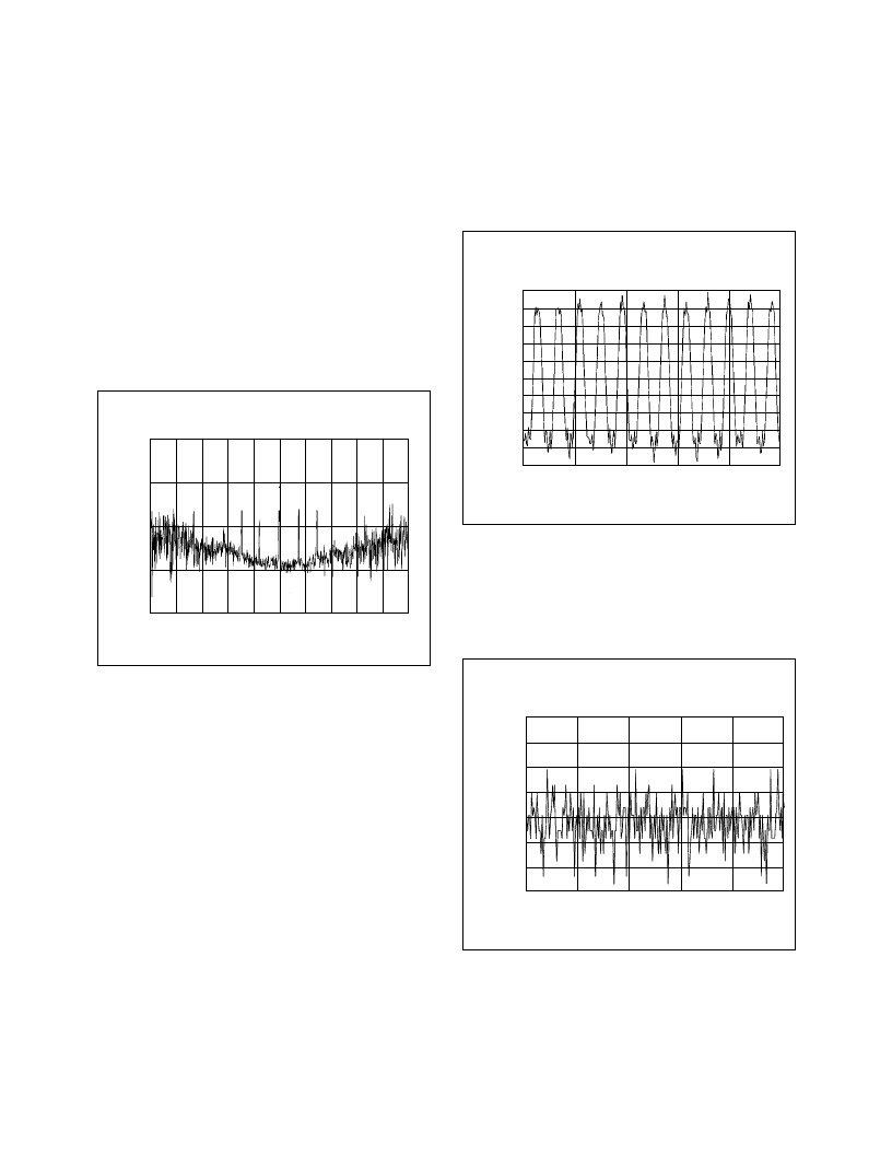
FIGURE 5. The noise shown in this graph is only apparent
after the noise levels of the ADS1210 and ADS1211 conver-
sion process has been reduced through techniques discussed
in this application. These techniques include proper pro-
gramming of the modulator, proper data rates, and proper
power plane layout.
FIGURE 6. The peaks shown in Figure 4 have a very low
frequency content. The frequency and magnitude of these
tones changes with layout and A/D converter programming
of turbo mode and data rate. This data was taken with the a
XIN of 10MHz, PGA of 1, decimation ratio of 195 and a
turbo mode of one.
ADS1210
TURBO 16, PGA 1, DR 3125, 100Hz, V
IN
= 0V
Samples
1
51
101
151
201
251
O
1.00E
0.00E
–1.00E
–2.00E
–3.00E
–4.00E
–5.00E
–6.00E
–7.00E
–8.00E
–9.00E
ADS1210
TURBO 16, PGA 1, DR 3125, 100Hz, SMALL INPUT
Samples
1
51
101
151
201
251
O
–2.22E
–2.24E
–2.26E
–2.28E
–2.30E
–2.32E
–2.34E
–2.36E
相關(guān)PDF資料 |
PDF描述 |
|---|---|
| AB-123 | AB-123 - USING THE CONTINUOUS PARALLEL MODE WITH THE ADS7824 AND ADS7825 |
| AB-124 | AB-124 - THD+N VERSUS FREQUENCY CHARACTERISTICS AND SPECTRA OF THE PCM1717 |
| AB-125 | AB-125 - CUSTOMIZING THE DDC112 EVALUATION FIXTURE |
| AB-127 | AB-127 - ADS121x ANALOG-DIGITAL CONVERTER APPLICATIONS PRIMER |
| AB-12 | Application Bulletin AB-12 |
相關(guān)代理商/技術(shù)參數(shù) |
參數(shù)描述 |
|---|---|
| AB122008 | 制造商:Fibox 功能描述:Bulk |
| AB1224DB-Y01 | 制造商:ADDA Corporation 功能描述:FAN WITH PLASTIC FRAME MATERIAL |
| AB1224HB-Y01 | 制造商:ADDA Corporation 功能描述:FAN WITH PLASTIC FRAME MATERIAL |
| AB1224HB-Y01-LF | 功能描述:鼓風(fēng)機(jī) 120mm 24VDC 25.2CFM RoHS:否 制造商:Murata 產(chǎn)品:Blowers 電流類型:DC 電源電壓:5.3 V 氣流:1 l/min 軸承類型: 噪聲: 速度: 功率額定值: 框架尺寸 (mm):20 mm x 20 mm x 1.85 mm 外殼材料: 端接類型:SMD/SMT 系列:MZB |
| AB1224LB-Y01 | 制造商:ADDA Corporation 功能描述:FAN WITH PLASTIC FRAME MATERIAL |
發(fā)布緊急采購,3分鐘左右您將得到回復(fù)。