- 您現(xiàn)在的位置:買賣IC網(wǎng) > PDF目錄373859 > AD1674T (Analog Devices, Inc.) 12-Bit 100 kSPS A/D Converter PDF資料下載
參數(shù)資料
| 型號: | AD1674T |
| 廠商: | Analog Devices, Inc. |
| 英文描述: | 12-Bit 100 kSPS A/D Converter |
| 中文描述: | 12位100 kSPS的A / D轉(zhuǎn)換 |
| 文件頁數(shù): | 7/12頁 |
| 文件大小: | 255K |
| 代理商: | AD1674T |
AD1674
REV. C
–7–
PIN DE SCRIPT ION
Symbol
Pin No.
T ype
Name and Function
AGND
A
0
9
4
P
DI
Analog Ground (Common).
Byte Address/Short Cycle. If a conversion is started with A
0
Active LOW, a full 12-bit conversion
cycle is initiated. If A
0
is Active HIGH during a convert start, a shorter 8-bit conversion cycle
results. During Read (R/
C
= 1) with 12/
8
LOW, A
0
= LOW enables the 8 most significant bits
(DB4–DB11), and A
0
= HIGH enables DB3–DB0 and sets DB7–DB4 = 0.
Bipolar Offset. Connect through a 50
resistor to REF OUT for bipolar operation or to Analog
Common for unipolar operation.
Chip Enable. Chip Enable is Active HIGH and is used to initiate a convert or read operation.
Chip Select. Chip Select is Active LOW.
Data Bits 11 through 8. In the 12-bit format (see 12/
8
and A
0
pins), these pins provide the up-
per 4 bits of data. In the 8-bit format, they provide the upper 4 bits when A
0
is LOW and are
disabled when A
0
is HIGH.
Data Bits 7 through 4. In the 12-bit format these pins provide the middle 4 bits of data. In the
8-bit format they provide the middle 4 bits when Ao is LOW and all zeroes when A
0
is HIGH.
Data Bits 3 through 0. In the 12-bit format these pins provide the lower 4 bits of data. In the
8-bit format these pins provide the lower 4 bits of data when A
0
is HIGH, they are disabled
when A
0
is LOW.
Digital Ground (Common).
+10 V Reference Output.
Read/Convert. In the full control mode R/
C
is Active HIGH for a read operation and Active LOW
for a convert operation. In the stand-alone mode, the falling edge of R/
C
initiates a conversion.
Reference Input is connected through a 50
resistor to +10 V Reference for normal operation.
Status is Active HIGH when a conversion is in progress and goes LOW when the conversion is
completed.
+12 V/+15 V Analog Supply.
–12 V/–15 V Analog Supply.
+5 V Logic Supply.
10 V Span Input, 0 V to +10 V unipolar mode or –5 V to +5 V bipolar mode. When using the
AD1674 in the 20 V Span 10 V
IN
should not be connected.
20 V Span Input, 0 V to +20 V unipolar mode or –10 V to +10 V bipolar mode. When using
the AD1674 in the 10 V Span 20 V
IN
should not be connected.
T he 12/
8
pin determines whether the digital output data is to be organized as two 8-bit words
(12/
8
LOW) or a single 12-bit word (12/
8
HIGH).
BIP OFF
12
AI
CE
CS
DB11–DB8
6
3
27–24
DI
DI
DO
DB7–DB4
23–20
DO
DB3–DB0
19–16
DO
DGND
REF OUT
R/
C
15
8
5
P
AO
DI
REF IN
ST S
10
28
AI
DO
V
CC
V
EE
V
LOGIC
10 V
IN
7
11
1
13
P
P
P
AI
20 V
IN
14
AI
12/
8
2
DI
T YPE:
AI
AO =
DI
DO =
P
=
Analog Input
Analog Output
Digital Input
Digital Output
Power
=
=
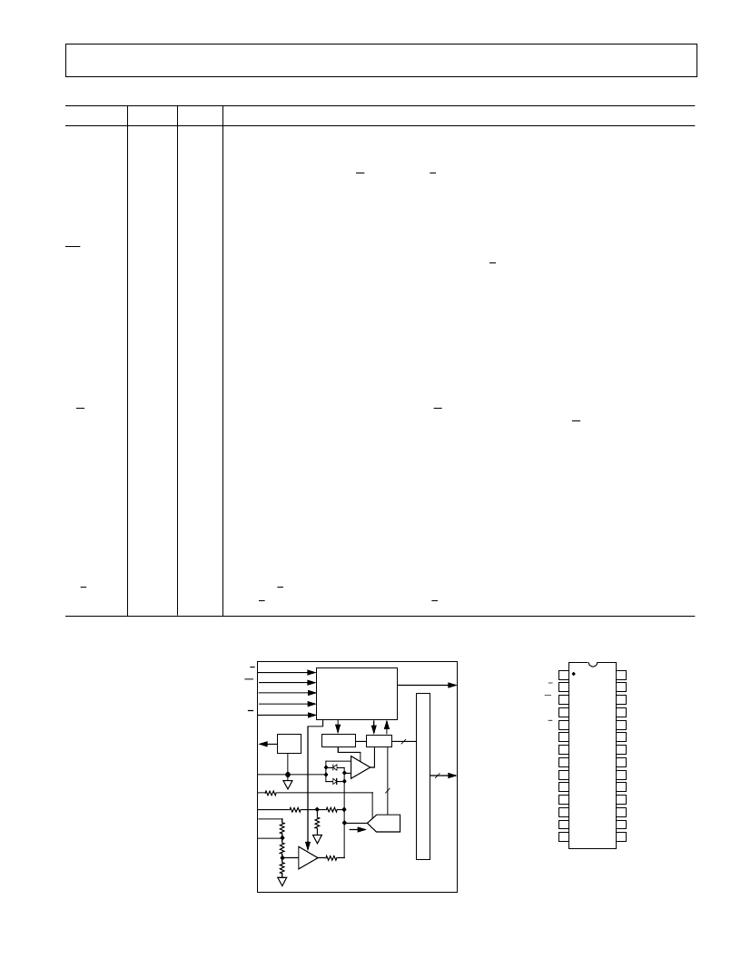
FUNCT IONAL BLOCK DIAGRAM
REF OUT
SHA
COMP
AA
20k
AAA
10k
5k
2.5k
2.5k
5k
12
AD1674
AGND
BIP OFF
20V
IN
REF IN
10V
IN
IDAC
12
CONTROL
CE
R/C
12/8
CS
A
0
5k
10k
AA
SAR
CLOCK
AAA
10V
A
A
A
A
A
A
R
DAC
STS
DB11 (MSB)
DB0 (LSB)
PIN CONFIGURAT ION
TOP VIEW
(Not to Scale)
AD1674
18
28
27
24
23
22
26
25
21
20
19
17
16
15
13
1
2
5
6
7
3
4
8
9
10
12
14
V
LOGIC
12/8
CE
V
CC
A
0
REF OUT
AGND
REF IN
V
EE
BIP OFF
10V
IN
20V
IN
CS
R/C
STS
DB11(MSB)
DB10
DB8
DB7
DB6
DB9
DB5
DB4
DB3
DB2
DB1
DB0(LSB)
DGND
11
相關(guān)PDF資料 |
PDF描述 |
|---|---|
| AD1674TD | 12-Bit 100 kSPS A/D Converter |
| AD1674* | 12-Bit 100 kSPS A/D Converter |
| AD1674 | 12-Bit 100 kSPS A/D Converter(12位100kSPS A/D轉(zhuǎn)換器) |
| AD1801 | Single-Chip Fax/Data/ Voice Modem(單片的傳真/數(shù)據(jù)/語音調(diào)制解調(diào)器) |
| AD1803JRU | U.S./International Modem DAA Line Codec Chipset |
相關(guān)代理商/技術(shù)參數(shù) |
參數(shù)描述 |
|---|---|
| AD1674TD | 功能描述:模數(shù)轉(zhuǎn)換器 - ADC 12-Bit 100 kSPS Complete IC RoHS:否 制造商:Analog Devices 通道數(shù)量: 結(jié)構(gòu): 轉(zhuǎn)換速率: 分辨率: 輸入類型: 信噪比: 接口類型: 工作電源電壓: 最大工作溫度: 安裝風(fēng)格: 封裝 / 箱體: |
| AD1674TD/883B | 功能描述:模數(shù)轉(zhuǎn)換器 - ADC 12-Bit 100 kSPS Complete IC RoHS:否 制造商:Analog Devices 通道數(shù)量: 結(jié)構(gòu): 轉(zhuǎn)換速率: 分辨率: 輸入類型: 信噪比: 接口類型: 工作電源電壓: 最大工作溫度: 安裝風(fēng)格: 封裝 / 箱體: |
| AD1679KD | 制造商:Analog Devices 功能描述: |
| AD16AA025 | 制造商:未知廠家 制造商全稱:未知廠家 功能描述:Logic IC |
| AD16AA050 | 制造商:未知廠家 制造商全稱:未知廠家 功能描述:Logic IC |
發(fā)布緊急采購,3分鐘左右您將得到回復(fù)。