- 您現(xiàn)在的位置:買(mǎi)賣(mài)IC網(wǎng) > PDF目錄373859 > AD1812 (Analog Devices, Inc.) SoundPort Controller(SoundPort控制器) PDF資料下載
參數(shù)資料
| 型號(hào): | AD1812 |
| 廠(chǎng)商: | Analog Devices, Inc. |
| 英文描述: | SoundPort Controller(SoundPort控制器) |
| 中文描述: | SoundPort控制器(SoundPort控制器) |
| 文件頁(yè)數(shù): | 5/20頁(yè) |
| 文件大?。?/td> | 314K |
| 代理商: | AD1812 |
第1頁(yè)第2頁(yè)第3頁(yè)第4頁(yè)當(dāng)前第5頁(yè)第6頁(yè)第7頁(yè)第8頁(yè)第9頁(yè)第10頁(yè)第11頁(yè)第12頁(yè)第13頁(yè)第14頁(yè)第15頁(yè)第16頁(yè)第17頁(yè)第18頁(yè)第19頁(yè)第20頁(yè)
AD1812
REV. 0
–5–
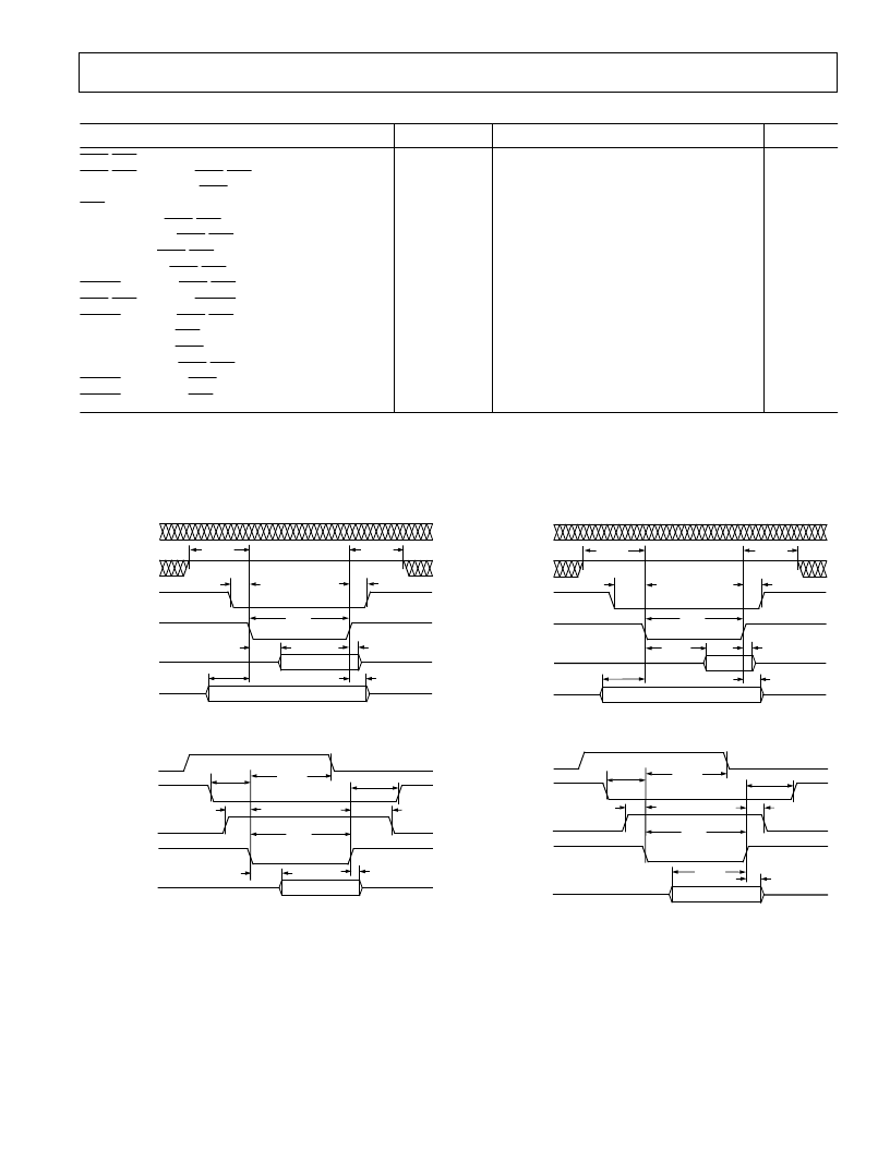
TIMING PARAMETERS (GUARANTEED OVER OPERATING TEMPERATURE RANGE)
Parameter
Symbol
Min
Typ
Max
Units
IOW
/
IOR
Strobe Width
IOW
/
IOR
Rising to
IOW
/
IOR
Falling
Write Data Setup to
IOW
Rising
IOR
Falling to Valid Read Data
AEN Setup to
IOW
/
IOR
Falling
AEN Hold from
IOW
/
IOR
Rising
Adr Setup to
IOW
/
IOR
Falling
Adr Hold from
IOW
/
IOR
Rising
DACK
Rising to
IOW
/
IOR
Falling
IOW
/
IOR
Rising to
DACK
Falling
DACK
Setup to
IOW
/
IOR
Falling
Data Hold from
IOR
Rising
Data Hold from
IOW
Rising
DRQ Hold from
IOW
/
IOR
Falling
DACK
Hold from
IOW
Rising
DACK
Hold from
IOR
Rising
t
STW
t
BWDN
t
WDSU
t
RDDV
t
AESU
t
AEHD
t
ADSU
t
ADHD
t
DKSU1
t
DKHD1
t
DKSU2
t
DHD1
t
DHD2
t
DRHD
t
DKHD2
t
DKHD3
100
80
10
ns
ns
ns
ns
ns
ns
ns
ns
ns
ns
ns
ns
ns
ns
ns
ns
40
10
0
10
10
20
0
10
20
15
25
10
10
*Guaranteed, not tested.
Specifications subject to change without notice.
General Notes
Use the exact timing information given. Do not attempt to derive parameters from the addition or subtraction of others. While addition or subtraction would yield
meaningful results for an additional device, the values given in this data sheet reflect statistical variations and worst cases. Consequently, you cannot meaningfully add
up parameters to derive longer times. Note that all 8-bit DMA transfers occur on channels 0, 1, and 3, while all 16-bit DMA transfers occur on channels 5, 6, and 7.
t
DKSU1
t
DKHD1
t
AESU
t
AEHD
t
STW
t
RDDV
t
DHD1
t
ADHD
t
ADSU
DRQ
(0, 1, 3, 5, 6, 7)
DACK
(0, 1, 3, 5, 6, 7)
AEN
IOR
PC_D (7:0) /
PC_D (15:0)
PC_A (15:0)
Figure 1. PIO Read Cycle
t
DKHD3
t
AESU
t
AEHD
t
RDDV
t
DHD1
t
DKSU2
t
DRHD
DRQ
(0, 1, 3, 5, 6, 7)
DACK
(0, 1, 3, 5, 6, 7)
AEN
IOR
PC_D (7:0) /
PC_D (15:0)
t
STW
Figure 3. DMA Read Cycle
t
DKSU1
t
DKHD1
t
AESU
t
AEHD
t
STW
t
DHD2
t
ADHD
DRQ
(0, 1, 3, 5, 6, 7)
DACK
(0, 1, 3, 5, 6, 7)
AEN
IOW
PC_D (7:0) /
PC_D (15:0)
PC_A (15:0)
t
ADSU
t
WDSU
Figure 2. PIO Write Cycle
t
DKHD2
t
AESU
t
AEHD
t
DHD2
t
DKSU2
t
DRHD
DRQ
(0, 1, 3, 5, 6, 7)
DACK
(0, 1, 3, 5, 6, 7)
AEN
IOW
PC_D (7:0) /
PC_D (15:0)
t
STW
t
WDSU
Figure 4. DMA Write Cycle
相關(guān)PDF資料 |
PDF描述 |
|---|---|
| AD1815 | SoundComm Controller(SoundComm 控制器) |
| AD1816AJS | SoundPort Controller |
| AD1816AJST | SoundPort Controller |
| AD1816A | SoundPort Controller(數(shù)字音頻的聲音端口控制器) |
| AD1818 | PCI SoundComm DC97 Digital Controller(PCI SoundComm DC97型數(shù)字控制器) |
相關(guān)代理商/技術(shù)參數(shù) |
參數(shù)描述 |
|---|---|
| AD1812AJS | 制造商:Analog Devices 功能描述: |
| AD1812JS | 制造商:AD 制造商全稱(chēng):Analog Devices 功能描述:SoundPort Controller |
| AD1812JST | 制造商:AD 制造商全稱(chēng):Analog Devices 功能描述:SoundPort Controller |
| AD1815 | 制造商:AD 制造商全稱(chēng):Analog Devices 功能描述:Sound Comm Controleer |
| AD1815JS | 制造商:Rochester Electronics LLC 功能描述:- Bulk 制造商:Analog Devices 功能描述: |
發(fā)布緊急采購(gòu),3分鐘左右您將得到回復(fù)。