- 您現(xiàn)在的位置:買賣IC網(wǎng) > PDF目錄373859 > AD1833ACST-REEL (ANALOG DEVICES INC) 24-Bit, 192 kHz, DAC PDF資料下載
參數(shù)資料
| 型號(hào): | AD1833ACST-REEL |
| 廠商: | ANALOG DEVICES INC |
| 元件分類: | DAC |
| 英文描述: | 24-Bit, 192 kHz, DAC |
| 中文描述: | SERIAL INPUT LOADING, 24-BIT DAC, PQFP48 |
| 封裝: | 1.40 MM HEIGHT, LOW PROFILE, PLASTIC, MS-026BBC, QFP-48 |
| 文件頁數(shù): | 15/20頁 |
| 文件大?。?/td> | 687K |
| 代理商: | AD1833ACST-REEL |
REV. 0
AD1833A
–15–
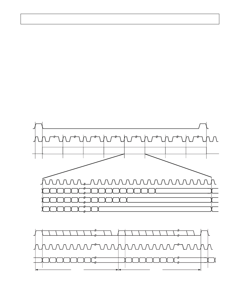
TDM Mode Timing—Interfacing to a SHARC
In TDM mode, the AD1833A can be the master or slave, depend-
ing on Bit 0 in Control Register 3. In master mode, it generates a
frame sync signal (FSTDM) on its L/RCLK pin and a bit clock
(BCLKTDM) on its BCLK pin, whereas in slave mode it expects
these signals to be provided. These signals are used to control
the data transmission from the SHARC. The bit clock must run
at a frequency of IMCLK/2 and the interpolation mode must be
set to 8 , which limits TDM mode to frequencies of 48 kHz or
less. In this mode, all data is written on the rising edge of the bit
clock and read on the falling edge of the bit clock. The frame
starts with a frame sync at the rising edge of the bit clock. The
SHARC then starts outputting data on the next rising edge of
the bit clock. Each channel is given a 32-bit clock slot, and the
data is left-justified and uses 16, 20, or 24 of the 32 bits. An
enlarged diagram detailing this is provided (see Figure 9). The
data is sent from the SHARC to the AD1833A on the SDIN1
pin and provided in the following order: MSB first—Internal
DACL0, Internal DACL1, Internal DACL2, AUX DACL0,
Internal DACR0, Internal DACR1, Internal DACR2, and AUX
DACR0. The data is written on the rising edge of the bit clock
and read by the AD1833A on the falling edge of the bit clock.
The left and right data destined for the auxiliary DAC is sent in
standard I
2
S format in the next frame using the SDIN2, SDIN3,
and SOUT pins as the L/RCLK, BCLK, and SDATA pins,
respectively, for communicating with the auxiliary DAC.
DSP Mode Timing
DSP mode timing uses the rising edge of the frame sync signal
on the L/RCLK pin to denote the start of the transmission of a
data-word. Note that for both left and right channels, a rising
edge is used; therefore in this mode, there is no way to determine
which data is intended for the left channel and which is intended
for the right. The DSP writes data on the rising edge of BCLK
and the AD1833A reads it on the falling edge. The DSP raises
the frame sync signal on the rising edge of BCLK and then proceeds
to transmit data, MSB first, on the next rising edge of BCLK.
The data length can be 16, 20, or 24 bits. The frame sync signal
can be brought low any time at or after the MSB is transmitted,
but must be brought low at least one BCLK period before the
start of the next channel transmission.
INTERNAL
DAC L0
INTERNAL
DAC L1
INTERNAL
DAC L2
AUXILIARY
DAC L0
INTERNAL
DAC R0
INTERNAL
DAC R1
INTERNAL
DAC R2
AUXILIARY
DAC R0
FSTDM
BCLKTDM
MSB
24-BIT DATA
20-BIT DATA
16-BIT DATA
BCLKTDM
–1
–2
–3
–4
+8
+7
+6
+5
+4
+3
+2
+1
LSB
MSB
–1
–2
–3
–4
+4
+3
+2
+1
LSB
MSB
–1
–2
–3
–4
LSB
Figure 9. TDM Mode Timing
L/RCLK
BCLK
SDATA
MSB
–1
–2
–4
–5
–6
MSB
–1
–2
–3
–4
–5
–6
MSB
32 BCLKs
32 BCLKs
–3
Figure 10. DSP Mode Timing
相關(guān)PDF資料 |
PDF描述 |
|---|---|
| AD1833AAST-REEL | 24-Bit, 192 kHz, DAC |
| AD1833 | Multichannel 24-Bit, 192 kHz, DAC |
| AD1833AST | Multichannel 24-Bit, 192 kHz, DAC |
| AD1835 | 2 ADC, 8 DAC, 96 kHz, 24-Bit Codec |
| AD1835AS | 2 ADC, 8 DAC, 96 kHz, 24-Bit Codec |
相關(guān)代理商/技術(shù)參數(shù) |
參數(shù)描述 |
|---|---|
| AD1833ACSTZ | 功能描述:IC DAC AUDIO 24BIT 6CH 48LQFP RoHS:是 類別:集成電路 (IC) >> 數(shù)據(jù)采集 - 數(shù)模轉(zhuǎn)換器 系列:- 標(biāo)準(zhǔn)包裝:2,400 系列:- 設(shè)置時(shí)間:- 位數(shù):18 數(shù)據(jù)接口:串行 轉(zhuǎn)換器數(shù)目:3 電壓電源:模擬和數(shù)字 功率耗散(最大):- 工作溫度:-40°C ~ 85°C 安裝類型:表面貼裝 封裝/外殼:36-TFBGA 供應(yīng)商設(shè)備封裝:36-TFBGA 包裝:帶卷 (TR) 輸出數(shù)目和類型:* 采樣率(每秒):* |
| AD1833AST | 制造商:Rochester Electronics LLC 功能描述:6 CHANNEL 24 BIT 192 KHZ DAC - Tape and Reel |
| AD1833AST-REEL | 制造商:Rochester Electronics LLC 功能描述:- Tape and Reel |
| AD1833CST | 制造商:Analog Devices 功能描述:DAC 6-CH Delta-Sigma 24-bit 48-Pin LQFP 制造商:Rochester Electronics LLC 功能描述:- Tape and Reel |
| AD1833CST-REEL | 制造商:Analog Devices 功能描述:DAC 6-CH Delta-Sigma 24-bit 48-Pin LQFP T/R 制造商:Rochester Electronics LLC 功能描述:- Tape and Reel |
發(fā)布緊急采購,3分鐘左右您將得到回復(fù)。