- 您現(xiàn)在的位置:買賣IC網(wǎng) > PDF目錄373859 > AD1835AS (ANALOG DEVICES INC) 2 ADC, 8 DAC, 96 kHz, 24-Bit Codec PDF資料下載
參數(shù)資料
| 型號(hào): | AD1835AS |
| 廠商: | ANALOG DEVICES INC |
| 元件分類: | 消費(fèi)家電 |
| 英文描述: | 2 ADC, 8 DAC, 96 kHz, 24-Bit Codec |
| 中文描述: | SPECIALTY CONSUMER CIRCUIT, PQFP52 |
| 封裝: | PLASTIC, MS-022AC, MQFP-52 |
| 文件頁(yè)數(shù): | 21/23頁(yè) |
| 文件大小: | 326K |
| 代理商: | AD1835AS |
第1頁(yè)第2頁(yè)第3頁(yè)第4頁(yè)第5頁(yè)第6頁(yè)第7頁(yè)第8頁(yè)第9頁(yè)第10頁(yè)第11頁(yè)第12頁(yè)第13頁(yè)第14頁(yè)第15頁(yè)第16頁(yè)第17頁(yè)第18頁(yè)第19頁(yè)第20頁(yè)當(dāng)前第21頁(yè)第22頁(yè)第23頁(yè)
REV. PrA
PRELIMINARY TECHNICAL DATA
AD1835
–21–
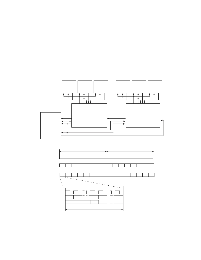
CASCADE MODE
Dual AD1835Cascade
The AD1835 can be cascaded to an additional AD1835 that,
in addition to six external stereo ADCs, can be used to create a
32-channel audio system with 16 inputs and 16 outputs. The
cascade is designed to connect to a SHARC DSP and operates
in a time division multiplexing (TDM) format. Figure 14
shows the connection diagram for cascade operation. The digital
interface for both parts must be set to operate in Auxiliary
512 mode by programming ADC Control Register II. AD1835
#1 is set as a master device by connecting the
M
/S pin to DGND,
and AD1835 #2 is set as a slave device by connecting the
M
/S to
DVDD. Both devices should be run from the same MCLK and
PD/RST
signals to ensure that they are synchronized.
With Device 1 set as a master, it will generate the frame-sync and
bit clock signals. These signals are sent to the SHARC and
Device 2 ensuring that both know when to send and receive data.
The cascade can be thought of as two 256-bit shift registers,
one for each device. At the beginning of a sample interval, the
shift registers contain the ADC results from the previous sample
interval. The first shift register (Device 1) clocks data into the
SHARC and also clocks in data from the second shift register
(Device 2). While this is happening, the SHARC is sending
DAC data to the second shift register. By the end of the sample
interval, all 512 bits of ADC data in the shift registers will have
been clocked into the SHARC and been replaced by DAC data
which is subsequently written to the DACs. Figure 15 shows
the timing diagram for the cascade operation.
AUX ADC
(SLAVE)
L
ALRCLK
ABCLK
ASDATA
DSDATA
ALRCLK
ABCLK
ASDATA
DSDATA
AD1835 #1
(MASTER)
AD1835 #2
(SLAVE)
SHARC
(SLAVE)
D
B
AUX ADC
(SLAVE)
L
D
B
AUX ADC
(SLAVE)
L
D
B
AUX ADC
(SLAVE)
L
D
B
AUX ADC
(SLAVE)
L
D
B
AUX ADC
(SLAVE)
L
D
B
A
A
A
A
A
A
A
A
A
A
DRx
RFSx
RCLKx
TCLKx
DTx
TFSx
Figure 14. Cascade
AD1835 #1 DACs
L1
L2
L3
L4
R1
R2
R3
R4
AD1835 #2 DACs
L1
L2
L3
L4
R1
R2
R3
R4
TFSx/
RFSx
DTx
AD1835 #1 ADCs
L1
L2
L3
L4
R1
R2
R3
R4
AD1835 #2 ADCs
L1
L2
L3
L4
R1
R2
R3
R4
DRx
256 ABCLKs
256 ABCLKs
MSB
MSB-1
LSB
32 ABCLKs
ABCLK
DTx
MSB
MSB-1
LSB
DRx
DON’T CARE
Figure 15. Cascade Timing
相關(guān)PDF資料 |
PDF描述 |
|---|---|
| AD1836ACSRL | Multichannel 96 kHz Codec |
| AD1836AAS | Multichannel 96 kHz Codec |
| AD1836AASRL | Direct-Conversion TV Tuner |
| AD1836ACS | Direct-Conversion TV Tuner |
| AD1836A | Multichannel 96 kHz Codec |
相關(guān)代理商/技術(shù)參數(shù) |
參數(shù)描述 |
|---|---|
| AD1835AS-REEL | 制造商:Analog Devices 功能描述:Audio Codec 2ADC / 8DAC 24-Bit 52-Pin MQFP T/R |
| AD1836 | 制造商:AD 制造商全稱:Analog Devices 功能描述:Multichannel 96 kHz Codec |
| AD1836A | 制造商:AD 制造商全稱:Analog Devices 功能描述:Multichannel 96 kHz Codec |
| AD1836AAS | 制造商:Analog Devices 功能描述:Audio Codec 2ADC / 3DAC 24-Bit 52-Pin MQFP 制造商:Rochester Electronics LLC 功能描述:MULTI CHANNEL 96 KHZ CODEC - Bulk 制造商:Analog Devices 功能描述:IC CODEC 96KHZ SMD 1836 MQFP52 |
| AD1836AASRL | 制造商:Analog Devices 功能描述:Audio Codec 2ADC / 3DAC 24-Bit 52-Pin MQFP T/R |
發(fā)布緊急采購(gòu),3分鐘左右您將得到回復(fù)。