- 您現(xiàn)在的位置:買賣IC網(wǎng) > PDF目錄373864 > AD1994ACPZRL7 (ANALOG DEVICES INC) Audio Switching Amplifier PDF資料下載
參數(shù)資料
| 型號: | AD1994ACPZRL7 |
| 廠商: | ANALOG DEVICES INC |
| 元件分類: | 音頻/視頻放大 |
| 英文描述: | Audio Switching Amplifier |
| 中文描述: | 25 W, 2 CHANNEL, AUDIO AMPLIFIER, QCC64 |
| 封裝: | 9 X 9 MM, LEAD FREE, MO-220VMMD-4, LFCSP-64 |
| 文件頁數(shù): | 18/24頁 |
| 文件大小: | 377K |
| 代理商: | AD1994ACPZRL7 |
AD1994
Output Transistor Nonoverlap Time
The AD1994 allows the user to select from one of eight different
nonoverlap times, as shown in Figure 46. Nonoverlap time
prevents or minimizes the period during which both the high-
side and low-side devices are on simultaneously due to propagation
delays and nonzero rise and fall times. If both the upper and
lower portions of a half-bridge conduct simultaneously, there is a
path directly from the power supply to ground and an induced
current flow known as shoot-through. However, introducing
this delay increases distortion by pushing the switching pattern
further from an ideal two-state waveform. Selecting the
nonoverlap delay requires a compromise between distortion
and efficiency. The logic levels on the three delay control pins,
DCTRL2, DCTRL1, and DCTRL0, set the nonoverlap time
according to
Table 12. The state of DCTRL[2:0] is read on the
rising edge of RESET and should not be changed while RESET
is logic high.
Rev. 0 | Page 18 of 24
Σ-Δ Modulator
As mentioned in the
a noise-shaping effect such that SNR is increased within the
audio band by shifting modulator quantization noise upward in
frequency. For external clock frequency of 12.288 MHz, the
modulator’s noise-shaping works in a manner that results in a
flat noise floor at the amplifier output for frequencies 20 kHz
and below. Above 20 kHz, the amplifier noise rises due to the
spectral shaping of the modulator quantization noise. At very
high frequencies, the noise floor levels off and decreases due to
poles in the modulator noise-transfer function and in the
external LC filter.
section, the modulator has
The clock frequency does not have to be exactly equal to
12.288 kHz and can vary by up to ±10%. For other rates, the
noise corner scales linearly with frequency. When the modulator
runs at a rate lower than nominal, the average power stage
switching frequency decreases, the efficiency increases slightly,
and the noise floor begins to rise at a slightly lower frequency.
Likewise, a faster clock gives slightly increased bandwidth and
slightly lower efficiency.
Table 12. Nonoverlap Time Settings
DCTRL2
DCTRL1
0
0
0
0
0
1
0
1
1
0
1
0
1
1
1
1
DCTRL0
0
1
0
1
0
1
0
1
Nonoverlap Time (ns)
1
62
49
37
24
15
13.5
12
9
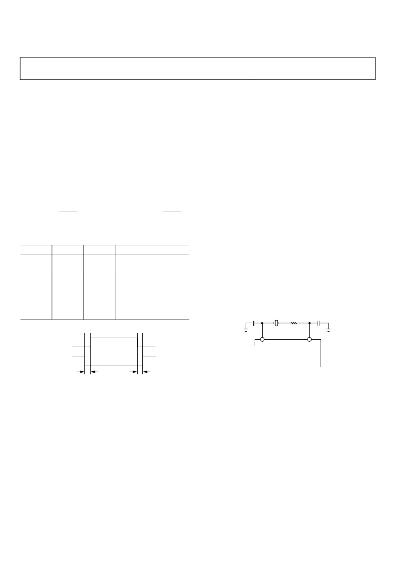
Using a Crystal Oscillator
The AD1994 can use a crystal connected to the CLKI and
CLKO pins as a master clock source, as shown in
CLKI and CLKO pins connect to an internal inverter to create a
full resonator. The typical values shown work in many applications,
but the crystal manufacturer should provide the exact type and
value of the capacitors and the resistor.
Figure 47. The
C
C
22pF
22pF
XTAL
47
0
Values are typical and are not production tested.
1
HIGH-SIDE
GATE DRIVE
LOW-SIDE
GATE DRIVE
t
NOL
t
NOL
0
Figure 47. Crystal Connection
Using an External Clock Source
If a clock signal of the appropriate frequency already exists in
the application circuit, connect it directly to CLKI and leave
CLKO floating. The logic levels of the square wave should be
compatible with those defined in
Figure 46. Half-Bridge Nonoverlap Delay Timing
The shortest setting (DCTRL[2:0] = 111) or the second shortest
setting (DCTRL[2:0] = 111) is recommended for most applications.
These two settings allow a small trade-off between efficiency
and distortion. Longer nonoverlap times generally increase
distortion while providing little or no decrease in shoot-
through current.
Specifications section.
Large amounts of jitter on the clock input degrade performance.
Whenever possible, avoid passing the clock signal though
programmable logic and other circuits with unknown or variable
propagation delay. In general, clock signals suitable for audio ADCs
or DACs are also appropriate for use with the AD1994.
CLOCKING
The AD1994 Σ-Δ modulator requires an external clock source
with a nominal frequency of 12.288 MHz. This clock can come
from a crystal or from an existing clock signal in the application
circuit. The discrete time portions of the modulator run internally
at 6.144 MHz, corresponding to 128 × f
, where f
S
S
= 48 kHz.
相關(guān)PDF資料 |
PDF描述 |
|---|---|
| AD203SN | Circular Connector; No. of Contacts:8; Series:LJTPQ00R; Body Material:Aluminum; Connecting Termination:Crimp; Connector Shell Size:17; Circular Contact Gender:Socket; Circular Shell Style:Wall Mount Receptacle |
| AD204 | Circular Connector; MIL SPEC:MIL-DTL-38999 Series I; Body Material:Metal; Series:LJT; No. of Contacts:11; Connector Shell Size:19; Connecting Termination:Crimp; Circular Shell Style:Wall Mount Receptacle; Body Style:Straight RoHS Compliant: No |
| AD204J | Circular Connector; MIL SPEC:MIL-DTL-38999 Series I; Body Material:Metal; Series:LJT; No. of Contacts:11; Connector Shell Size:19; Connecting Termination:Crimp; Circular Shell Style:Wall Mount Receptacle; Body Style:Straight RoHS Compliant: No |
| AD204JN | Circular Connector; No. of Contacts:28; Series:LJTPQ00R; Body Material:Aluminum; Connecting Termination:Crimp; Connector Shell Size:19; Circular Contact Gender:Socket; Circular Shell Style:Wall Mount Receptacle |
| AD204JY | Circular Connector; MIL SPEC:MIL-DTL-38999 Series I; Body Material:Metal; Series:LJT; No. of Contacts:32; Connector Shell Size:19; Connecting Termination:Crimp; Circular Shell Style:Wall Mount Receptacle; Body Style:Straight RoHS Compliant: No |
相關(guān)代理商/技術(shù)參數(shù) |
參數(shù)描述 |
|---|---|
| AD1994XCPZ | 制造商:Analog Devices 功能描述: |
| AD1996 | 制造商:Analog Devices 功能描述:IC, 12-BIT 1.25 MSPS ADC - Rail/Tube |
| AD1996ACPZ | 制造商:AD 制造商全稱:Analog Devices 功能描述:Class-D Audio Power Amplifier |
| AD-1999-TEMP-MEAS-RFLT | 制造商:TE Connectivity 功能描述: |
| AD19T | 制造商:Opto 22 功能描述:STANDARD (G1) I/O MODULES AND MOUNTING RACKS NIFNA |
發(fā)布緊急采購,3分鐘左右您將得到回復(fù)。