- 您現(xiàn)在的位置:買賣IC網(wǎng) > PDF目錄373870 > AD5203AR100 (ANALOG DEVICES INC) 4-Channel, 64-Position Digital Potentiometer PDF資料下載
參數(shù)資料
| 型號: | AD5203AR100 |
| 廠商: | ANALOG DEVICES INC |
| 元件分類: | 數(shù)字電位計(jì) |
| 英文描述: | 4-Channel, 64-Position Digital Potentiometer |
| 中文描述: | 100K DIGITAL POTENTIOMETER, 3-WIRE SERIAL CONTROL INTERFACE, 64 POSITIONS, PDSO24 |
| 封裝: | SOIC-24 |
| 文件頁數(shù): | 3/12頁 |
| 文件大小: | 259K |
| 代理商: | AD5203AR100 |
–3–
REV. 0
AD5203
NOTES
1
Typicals represent average readings at +25
°
C and V
= +5 V.
2
Resistor position nonlinearity error R-INL is the deviation from an ideal value measured between the maximum resistance and the minimum resistance wiper posi-
tions. R-DNL measures the relative step change from ideal between successive tap positions. Parts are guaranteed monotonic. See Figure 27 test circuit. I
W
= V
DD
/R
for both V
DD
= +3 V or V
= +5 V.
3
V
= V
) = No connect.
4
INL and DNL are measured at V
with the RDAC configured as a potentiometer divider similar to a voltage output D/A converter. V
A
= V
DD
and V
B
= 0 V.
DNL specification limits of
±
1 LSB maximum are guaranteed monotonic operating conditions. See Figure 26 test circuit.
5
Resistor terminals A, B, W have no limitations on polarity with respect to each other.
6
Guaranteed by design and not subject to production test.
7
Measured at the AX terminals. All AX terminals are open-circuited in shutdown mode.
8
Worst case supply current consumed when all logic-input levels set at 2.4 V, standard characteristic of CMOS logic. See Figure 19 for a plot of I
DD
vs. logic voltage
inputs result in minimum power dissipation.
9
P
is calculated from (I
×
V
DD
). CMOS logic level inputs result in minimum power dissipation.
10
All dynamic characteristics use V
= +5 V.
11
Measured at a V
pin where an adjacent V
pin is making a full-scale voltage change.
12
See timing diagrams for location of measured values. All input control voltages are specified with t
= t
= 1 ns (10% to 90% of V
) and timed from a voltage level
of 1.6 V. Switching characteristics are measured using both V
= +3 V or +5 V. Input logic should have a 1 V/
μ
s minimum slew rate.
13
Propagation delay depends on value of V
DD
, R
L
and C
L
. See Operation section.
ABSOLUTE MAXIMUM RATINGS*
(T
A
= +25
°
C, unless otherwise noted)
V
DD
to GND . . . . . . . . . . . . . . . . . . . . . . . . . . . .–0.3 V, +8 V
V
A
, V
B
, V
W
to GND . . . . . . . . . . . . . . . . . . . . . . . . . . 0 V, V
DD
I
AB
, I
AW
, I
BW
. . . . . . . . . . . . . . . . . . . . . . . . . . . . . . .
±
20 mA
Digital Input and Output Voltage to GND . . . . . . . 0 V, +8 V
Operating Temperature Range . . . . . . . . . . . –40
°
C to +85
°
C
Maximum Junction Temperature (T
J
MAX) . . . . . . . .+150
°
C
Storage Temperature . . . . . . . . . . . . . . . . . . –65
°
C to +150
°
C
Lead Temperature (Soldering, 10 sec) . . . . . . . . . . . .+300
°
C
Package Power Dissipation . . . . . . . . . . . . . . (T
J
max–T
A
)/
θ
JA
Thermal Resistance
θ
JA
P-DIP (N-24) . . . . . . . . . . . . . . . . . . . . . . . . . . . . 63
°
C/W
SOIC (SOL-24) . . . . . . . . . . . . . . . . . . . . . . . . . . . 70
°
C/W
TSSOP-24 . . . . . . . . . . . . . . . . . . . . . . . . . . . . . . 143
°
C/W
*Stresses above those listed under Absolute Maximum Ratings may cause perma-
nent damage to the device. This is a stress rating only; functional operation of the
device at these or any other conditions above those indicated in the operational
sections of this specification is not implied. Exposure to absolute maximum rating
conditions for extended periods may affect device reliability.
Table I. Serial-Data Word Format
ADDR
B7
DATA
B5
B6
B4
B3
B2
B1
B0
A1
MSB
2
7
A0
LSB
2
6
D5
MSB
2
5
D4
D3
D2
D1
D0
LSB
2
0
CAUTION
ESD (electrostatic discharge) sensitive device. Electrostatic charges as high as 4000 V readily
accumulate on the human body and test equipment and can discharge without detection.
Although the AD5203 features proprietary ESD protection circuitry, permanent damage may
occur on devices subjected to high energy electrostatic discharges. Therefore, proper ESD
precautions are recommended to avoid performance degradation or loss of functionality.
WARNING!
ESD SENSITIVE DEVICE
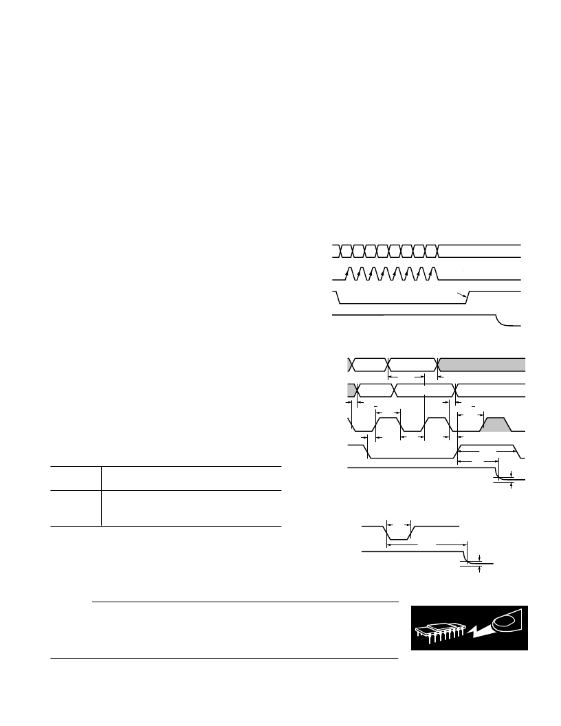
SDI
CLK
CS
V
OUT
1
0
1
0
1
0
V
DD
0V
D0
D1
D2
D3
D4
D5
A0
A1
DAC REGISTER LOAD
Figure 1a. Timing Diagram
CLK
V
OUT
1
0
1
0
1
0
V
DD
0V
SDI
(DATA IN)
SDO
(DATA OUT)
CS
1
0
Ax OR Dx
Ax OR Dx
A'x OR D'x
t
DS
t
DH
t
PD MAX
t
PD MIN
t
CH
t
CS1
t
CL
t
CSS
t
CSH
6
1 LSB
6
1 LSB ERROR BAND
t
t
S
A'x OR D'x
Figure 1b. Detail Timing Diagram
V
OUT
V
DD
0V
RS
1
0
6
1 LSB
6
1 LSB ERROR BAND
t
S
t
RS
Figure 1c. Reset Timing Diagram
相關(guān)PDF資料 |
PDF描述 |
|---|---|
| AD5203ARU10 | ECONOLINE: RO & RE - Industry Standard Pinout- 1kVDC & 2kVDC Isolation- UL94V-0 Package Material- Toroidal Magnetics- Fully Encapsulated- Custom Solutions Available- Efficiency to 85% |
| AD5203ARU100 | 4-Channel, 64-Position Digital Potentiometer |
| AD5206BR10 | 32-Tap. Nonvolatile. Linear-Taper Digital Potentiometers in SOT23 |
| AD5206BR100 | 32-Tap. Nonvolatile. Linear-Taper Digital Potentiometers in SOT23 |
| AD5206BR50 | 32-Tap. Nonvolatile. Linear-Taper Digital Potentiometers in SOT23 |
相關(guān)代理商/技術(shù)參數(shù) |
參數(shù)描述 |
|---|---|
| AD5203AR100-REEL | 制造商:Analog Devices 功能描述:Digital Potentiometer 64POS 100KOhm Quad 24-Pin SOIC W T/R 制造商:Rochester Electronics LLC 功能描述:QUAD 6-BIT POTENTIOMETER - Tape and Reel |
| AD5203AR10-REEL | 制造商:Analog Devices 功能描述:Digital Potentiometer 64POS 10KOhm Quad 24-Pin SOIC W T/R 制造商:Rochester Electronics LLC 功能描述:- Tape and Reel |
| AD5203ARU10 | 制造商:Rochester Electronics LLC 功能描述: 制造商:Analog Devices 功能描述: |
| AD5203ARU100 | 制造商:Rochester Electronics LLC 功能描述:QUAD 6-BIT POTENTIOMETER - Bulk |
| AD5203ARU100-REEL | 制造商:Rochester Electronics LLC 功能描述:- Tape and Reel |
發(fā)布緊急采購,3分鐘左右您將得到回復(fù)。