- 您現(xiàn)在的位置:買賣IC網(wǎng) > PDF目錄373886 > AD6122ACPRL (ANALOG DEVICES INC) CDMA 3 V Transmitter IF Subsystem with Integrated Voltage Regulator PDF資料下載
參數(shù)資料
| 型號: | AD6122ACPRL |
| 廠商: | ANALOG DEVICES INC |
| 元件分類: | 通信及網(wǎng)絡 |
| 英文描述: | CDMA 3 V Transmitter IF Subsystem with Integrated Voltage Regulator |
| 中文描述: | SPECIALTY TELECOM CIRCUIT, PQCC32 |
| 封裝: | MO-220-VHHD-2, LPCC-32 |
| 文件頁數(shù): | 12/20頁 |
| 文件大小: | 264K |
| 代理商: | AD6122ACPRL |
REV. B
AD6122
–
12
–
The AD6122’s overall gain, expressed in decibels, is linear in
dB with respect to the automatic gain control (AGC) voltage,
VGAIN. Either REFOUT or an external reference voltage con-
nected to REFIN may be used to set the voltage range for VGAIN.
When the internal 1.23 V reference, REFOUT, is connected to
REFIN , VGAIN will control the entire AGC range when it is
typically set between 0.5 V and 2.5 V. Minimum gain occurs at
minimum voltage on VGAIN and maximum gain occurs at maxi-
mum voltage on VGAIN. The maximum and minimum gain
will not change with a change in voltage at REFIN. Rather, the
slope of the gain curve will change as a result of a change in the
required range for VGAIN. Figure 24 shows the piecewise linear
approximation of the gain curve for the AD6122.
MINIMUM
GAIN
MAXIMUM
GAIN
G
–
VGAIN
–
V
Figure 24. Piecewise Linear Approximation for the
AD6122 Gain Curve
Because the minimum and maximum gain from the AD6122
are constant, we can approximate the VGAIN range for a
given REFIN voltage by using Equation 1.
VGAIN
GAIN
(
MinGain
MaxGain
REFIN
MinGain
REFIN
=
×
+
–
)
.
–
.
1 6
0 4
(1)
Where
MaxGain
is the maximum gain (+34 dB) in dB,
MinGain
is the minimum gain (
–
63 dB) in dB,
REFIN
is the reference
input voltage, in volts,
VGAIN
is the gain control voltage input,
in volts, and
GAIN
is the particular gain, in dB, we would have
for a given REFIN and VGAIN. Consequently, for any REFIN
we choose, we can calculate the VGAIN range by solving
Equation 1 for VGAIN. For example, in order to determine the
VGAIN value for the maximum gain condition, given a 1.23 V
REFIN, we can solve Equation 1 for VGAIN by substituting
+34 dB for GAIN and MaxGain,
–
63 dB for MinGain and 1.23 V
for REFIN. VGAIN can then be calculated to be 2.46 V, or
approximately 2.5 V. For the minimum gain condition, we can
determine the VGAIN value by substituting 34 dB for MaxGain,
–
63 dB for GAIN and MinGain and 1.23 V for REFIN. VGAIN
can then be calculated to be 0.492 V or approximately 0.5 V.
Power-Down Control
The AD6122 can be operated with the IF amplifiers and quadra-
ture modulator both powered up, both powered down or with
the IF amplifiers powered up and the modulator powered down.
The AD6122 cannot operate with only the modulator powered
up. The control is provided via two control pins, PD1 and PD2.
Table I shows the operating modes of the AD6122.
Table I. Operating Modes
PD1
PD2
IF Amp
Modulator
0
0
1
1
0
1
0
1
ON
ON
INVALID STATE
OFF
ON
OFF
INVALID STATE
OFF
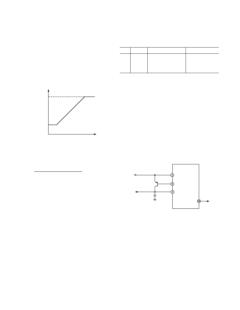
Low Dropout Regulator
The AD6122 incorporates an integrated low dropout regulator.
The regulator accepts inputs from 2.9 V to 4.2 V and supplies a
constant 2.7 V reference output at LDOC. The 2.7 V signal can
be used to provide the dc voltages required for the DVCC,
TXVCC and IFVCC dc supplies. In order to configure the low
dropout regulator, an external pass transistor is required. A pnp
bipolar junction transistor with a minimum h
FE
of 100 and a
maximum h
FE
of 300 and a VCE
SAT
of
–
0.4 V is required. In
order to use the low dropout regulator, configure the transistor as
shown in Figure 25. The 18 pF capacitor in Figure 25 is used for
decoupling the 2.7 V dc signal.
In addition to the low dropout regulator, a band-gap voltage
reference produces a 1.23 V reference voltage at REFOUT.
This reference voltage will be present whenever a 2.7 V dc sig-
nal is present on pin LDOC. This 1.23 V reference voltage can
then be used to provide the gain reference signal required for
REFIN and the reference voltage for the transmit DACs in a
baseband converter.
AD6122
LDOE
LDOC
LDOB
18pF
2.9V
–
4.2V
2.7V
REFOUT
1.23V
PASS
TRANSISTOR
Figure 25. Configuring the Low Dropout Regulator
It is possible to bypass the low dropout regulator on the AD6122
and use an external regulator instead. In order to bypass the
integrated low dropout regulator, connect pins LDOE, LDOB
and LDOC together and then connect them all to the 2.7 V
external regulator voltage. This configuration is shown in
Figure 26. Even when the low dropout regulator is bypassed,
the 1.23 V reference voltage at pin REFOUT is still present.
相關PDF資料 |
PDF描述 |
|---|---|
| AD6122 | CDMA 3 V Receiver IF Subsystem with Integrated Voltage Regulator(低功耗接收中頻子系統(tǒng)) |
| AD6140ARSRL | Bandpass IF Subsystem |
| AD6140ARS | RE Series - Econoline Unregulated DC-DC Converters; Input Voltage (Vdc): 3.3V; Output Voltage (Vdc): 12V; Power: 1W; Industry Standard Pinout; 1kVDC & 2kVDC Isolation; UL94V-0 Package Material; Optional Continuous Short Circuit Protected; Fully Encapsulated; Custom Solutions Available; Efficiency to 85% |
| AD6140 | Bandpass ∑△ IF Subsystem(帶通∑△IF子系統(tǒng)) |
| AD6190ARSRL | 900 MHz RF Transceiver |
相關代理商/技術(shù)參數(shù) |
參數(shù)描述 |
|---|---|
| AD6122ARS | 制造商:AD 制造商全稱:Analog Devices 功能描述:CDMA 3 V Transmitter IF Subsystem with Integrated Voltage Regulator |
| AD6122ARSRL | 制造商:AD 制造商全稱:Analog Devices 功能描述:CDMA 3 V Transmitter IF Subsystem with Integrated Voltage Regulator |
| AD612BS | 制造商:POP 功能描述: |
| AD6140 | 制造商:AD 制造商全稱:Analog Devices 功能描述:Bandpass IF Subsystem |
| AD6140ARS | 制造商:Rochester Electronics LLC 功能描述:- Bulk |
發(fā)布緊急采購,3分鐘左右您將得到回復。