- 您現(xiàn)在的位置:買賣IC網(wǎng) > PDF目錄373889 > AD645KN (ANALOG DEVICES INC) Low Noise, Low Drift FET Op Amp PDF資料下載
參數(shù)資料
| 型號(hào): | AD645KN |
| 廠商: | ANALOG DEVICES INC |
| 元件分類: | 運(yùn)動(dòng)控制電子 |
| 英文描述: | Low Noise, Low Drift FET Op Amp |
| 中文描述: | OP-AMP, 400 uV OFFSET-MAX, 2 MHz BAND WIDTH, PDIP8 |
| 封裝: | PLASTIC, DIP-8 |
| 文件頁數(shù): | 8/8頁 |
| 文件大小: | 439K |
| 代理商: | AD645KN |
AD645
REV. B
–8–
C
P
V = I Rf
PHOTODIODE
AD645
10pF
V
OUT
R
G
10k
10
8
Rf
1.1k
R
i
R
G
R
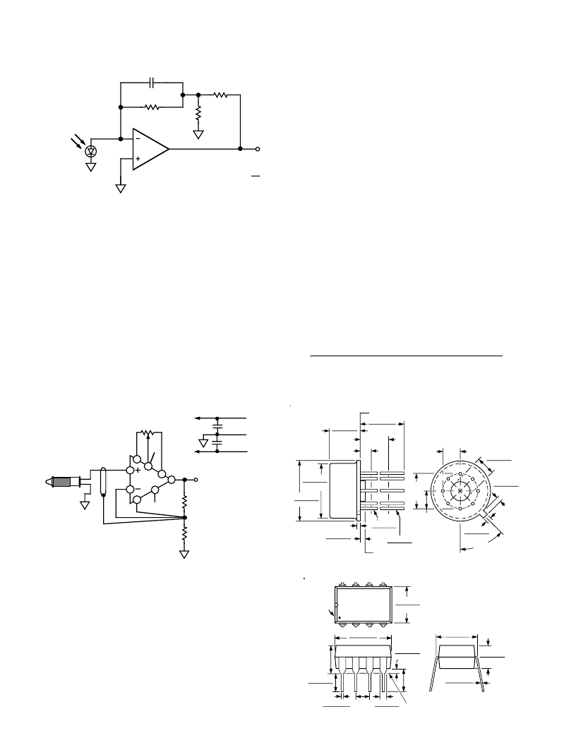
Figure 34. A Photodiode Preamp Employing a “T”
Network for Added Gain
A pH Probe Buffer Amplifier
A typical pH probe requires a buffer amplifier to isolate its 10
6
to 10
9
source resistance from external circuitry. Just such an
amplifier is shown in Figure 35. The low input current of the
AD645 allows the voltage error produced by the bias current
and electrode resistance to be minimal. The use of guarding,
shielding, high insulation resistance standoffs, and other such
standard methods used to minimize leakage are all needed to
maintain the accuracy of this circuit.
The slope of the pH probe transfer function, 50 mV per pH unit
at room temperature, has a +3300 ppm/
°
C temperature coeffi-
cient. The buffer of Figure 35 provides an output voltage equal
to 1 volt/pH unit. Temperature compensation is provided by
resistor RT which is a special temperature compensation resis-
tor, part number Q81, 1 k
, 1%, +3500 ppm/
°
C, available from
Tel Labs Inc.
GUARD
8
1
4
6
7
3
2
5
AD645
V
S
–
V ADJUST
100k
pH
PROBE
V
+
S
OUTPUT
1VOLT/pH UNIT
19.6k
RT
1k
+3500ppm/
°
C
0.1
μ
F
0.1
μ
F
+15V
COM
–15V
–V
S
+V
S
Figure 35. A pH Probe Amplifier
Circuit Board Notes
The AD645 is designed for through hole mount into PC boards.
Maintaining picoampere level resolution in that environment
requires a lot of care. Since both the printed circuit board and
the amplifier’s package have a finite resistance, the voltage dif-
ference between the amplifier’s input pin and other pins (or
traces on the PC board) will cause parasitic currents to flow into
(or out of) the signal path. These currents can easily exceed the
1.5 pA input current level of the AD645 unless special precau-
tions are taken. Two successful methods for minimizing leakage
are: guarding the AD645’s input lines and maintaining adequate
insulation resistance.
Guarding the input lines by completely surrounding them with a
metal conductor biased near the input lines’ potential has two
major benefits. First, parasitic leakage from the signal line is
reduced, since the voltage between the input line and the guard
is very low. Second, stray capacitance at the input terminal is
minimized which in turn increases signal bandwidth. In the
header or can package, the case of the AD645 is connected to
Pin 8 so that it may be tied to the input potential (when operat-
ing as a follower) or tied to ground (when operating as an in-
verter). The AD645’s positive input (Pin 3) is located next to
the negative supply voltage pin (Pin 4). The negative input (Pin
2) is next to the balance adjust pin (Pin 1) which is biased at a
potential close to that of the negative supply voltage. Note that
any guard traces should be placed on
both
sides of the board. In
addition, the input trace should be guarded along both of its
edges, along its entire length.
Contaminants such as solder flux, on the board’s surface and on
the amplifier’s package, can greatly reduce the insulation resis-
tance and also increase the sensitivity to atmospheric humidity.
Both the package and the board must be kept clean and dry. An
effective cleaning procedure is to: first, swab the surface with
high grade isopropyl alcohol, then rinse it with deionized water,
and finally, bake it at 80
°
C for 1 hour. Note that if either poly-
styrene or polypropylene capacitors are used on the printed cir-
cuit board that a baking temperature of 70
°
C is safer, since both
of these plastic compounds begin to melt at approximately
+85
°
C.
OUTLINE DIMENSIONS
Dimensions shown in inches and (mm).
TO-99 Header (H) Package
°
45
0.100
(2.54)
BSC
0.034 (0.86)
0.027 (0.69)
0.045 (1.14)
0.027 (0.69)
0.160 (4.06)
0.110 (2.79)
0.100
(2.54)
BSC
0.200
(5.08)
BSC
6
8
5
7
1
4
2
3
REFERENCE PLANE
0.750 (19.05)
0.500 (12.70)
BASE & SEATING PLANE
0.335 (8.51)
0.305 (7.75)
0.370 (9.40)
0.335 (8.51)
0.045 (1.14)
0.010 (0.25)
0.050
(1.27)
MAX
0.040 (1.02) MAX
0.019 (0.48)
0.016 (0.41)
0.021 (0.53)
0.016 (0.41)
0.185 (4.70)
0.165 (4.19)
0.250 (6.35)
MIN
Plastic Mini-DIP (N) Package
PIN 1
0.280 (7.11)
0.240 (6.10)
4
5
8
1
SEATING
PLANE
0.060 (1.52)
0.015 (0.38)
0.130
(3.30)
MIN
0.210
(5.33)
MAX
0.160 (4.06)
0.115 (2.93)
0.430 (10.92)
0.348 (8.84)
0.022 (0.558)
0.014 (0.356)
0.070 (1.77)
0.045 (1.15)
0.100
(2.54)
BSC
0.325 (8.25)
0.300 (7.62)
0.015 (0.381)
0.008 (0.204)
0.195 (4.95)
0.115 (2.93)
相關(guān)PDF資料 |
PDF描述 |
|---|---|
| AD645S | Low Noise, Low Drift FET Op Amp |
| AD645A | Low Noise, Low Drift FET Op Amp |
| AD645AH | Low Noise, Low Drift FET Op Amp |
| AD645B | Low Noise, Low Drift FET Op Amp |
| AD645BH | Low Noise, Low Drift FET Op Amp |
相關(guān)代理商/技術(shù)參數(shù) |
參數(shù)描述 |
|---|---|
| AD645S | 制造商:AD 制造商全稱:Analog Devices 功能描述:Low Noise, Low Drift FET Op Amp |
| AD645SH | 制造商:未知廠家 制造商全稱:未知廠家 功能描述:Operational Amplifier |
| AD645SH/883B | 制造商:AD 制造商全稱:Analog Devices 功能描述:Low Noise, Low Drift FET Op Amp |
| AD647 | 制造商:AD 制造商全稱:Analog Devices 功能描述:Ultralow Drift, Dual BiFET Op Amp |
| AD6472 | 制造商:AD 制造商全稱:Analog Devices 功能描述:2 Pair/1 Pair ETSI Compatible HDSL Analog Front End |
發(fā)布緊急采購,3分鐘左右您將得到回復(fù)。