- 您現(xiàn)在的位置:買賣IC網 > PDF目錄373891 > AD6645ASQ-80 (ANALOG DEVICES INC) 14-Bit, 80 MSPS A/D Converter PDF資料下載
參數(shù)資料
| 型號: | AD6645ASQ-80 |
| 廠商: | ANALOG DEVICES INC |
| 元件分類: | ADC |
| 英文描述: | 14-Bit, 80 MSPS A/D Converter |
| 中文描述: | 1-CH 14-BIT PROPRIETARY METHOD ADC, PARALLEL ACCESS, PQFP52 |
| 封裝: | POWER, MS-026BCCHD, LQFP-52 |
| 文件頁數(shù): | 14/20頁 |
| 文件大?。?/td> | 2230K |
| 代理商: | AD6645ASQ-80 |
REV. 0
AD6645
–14–
THEORY OF OPERATION
The AD6645 analog-to-digital converter (ADC) employs a three
stage subrange architecture. This design approach achieves the
required accuracy and speed while maintaining low power and
small die size.
As shown in the functional block diagram, the AD6645 has
complementary analog input pins, AIN and
AIN
. Each analog
input is centered at 2.4 V and should swing
±
0.55 V around this
reference (see Figure 2). Since AIN and
AIN
are 180 degrees out
of phase, the differential analog input signal is 2.2 V
peak-to-peak.
Both analog inputs are buffered prior to the first track-and-hold,
TH1. The high state of the ENCODE pulse places TH1 in hold
mode. The held value of TH1 is applied to the input of a 5-bit
coarse ADC1. The digital output of ADC1 drives a 5-bit digital-
to-analog converter, DAC1. DAC1 requires 14 bits of precision,
which is achieved through laser trimming. The output of DAC1
is subtracted from the delayed analog signal at the input of TH3
to generate a first residue signal. TH2 provides an analog pipe-
line delay to compensate for the digital delay of ADC1.
The first residue signal is applied to a second conversion stage
consisting of a 5-bit ADC2, 5-bit DAC2, and pipeline TH4.
The second DAC requires 10 bits of precision, which is met
by the process with no trim. The input to TH5 is a second resi-
due signal generated by subtracting the quantized output of
DAC2 from the first residue signal held by TH4. TH5 drives
a final 6-bit ADC3.
The digital outputs from ADC1, ADC2, and ADC3 are added
together and corrected in the digital error correction logic to
generate the final output data. The result is a 14-bit parallel
digital CMOS-compatible word, coded as two
’
s complement.
APPLYING THE AD6645
Encoding the AD6645
The AD6645 encode signal must be a high quality, extremely
low phase noise source to prevent degradation of performance.
Maintaining 14-bit accuracy places a premium on encode clock
phase noise. SNR performance can easily degrade by 3
–
4 dB
with 70 MHz analog input signals when using a high jitter clock
source. See AN-501,
“
Aperture Uncertainty and ADC System
Performance
”
for complete details.
For optimum performance, the AD6645 must be clocked differ-
entially. The encode signal is usually ac-coupled into the ENC
and
ENC
pins via a transformer or capacitors. These pins are
biased internally and require no additional bias.
Shown below is one preferred method for clocking the AD6645.
The clock source (low jitter) is converted from single-ended to
differential using a RF transformer. The back-to-back Schottky
diodes across the transformer secondary limit clock excursions
into the AD6645 to approximately 0.8 V p-p differential. This
helps prevent the large voltage swings of the clock from feeding
through to other portions of the AD6645, and limits the noise
presented to the encode inputs.
ENCODE
ENCODE
0.1 F
T1-4T
HSMS2812
DIODES
AD6645
CLOCK
SOURCE
Figure 8. Crystal Clock Oscillator, Differential Encode
If a low jitter clock is available, another option is to ac-couple a
differential ECL/PECL signal to the encode input pins as shown
below. The MC100EL16 (or same family) from ON-SEMI
offers excellent jitter performance.
ENCODE
ENCODE
AD6645
VT
VT
0.1 F
0.1 F
ECL/
PECL
Figure 9. Differential ECL for Encode
Driving the Analog Inputs
As with most new high-speed, high dynamic range analog-to-
digital converters, the analog input to the AD6645 is differential.
Differential inputs improve on-chip performance as signals are
processed through attenuation and gain stages. Most of the
improvement is a result of differential analog stages having high
rejection of even-order harmonics. There are also benefits at the
PCB level. First, differential inputs have high common-mode
rejection to stray signals such as ground and power noise. Sec-
ond, they provide good rejection to common-mode signals such
as local oscillator feed-through.
The AD6645 analog input voltage range is offset from ground by
2.4 V. Each analog input connects through a 500
W
resistor to the
2.4 V bias voltage and to the input of a differential buffer (Fig-
ure 2). The resistor network on the input properly biases the
followers for maximum linearity and range. Therefore, the analog
source driving the AD6645 should be ac-coupled to the input
pins. Since the differential input impedance of the AD6645 is 1 k
W
,
the analog input power requirement is only
–
2 dBm, simplifying
the driver amplifier in many cases. To take full advantage of this
high input impedance, a 20:1 transformer would be required.
This is a large ratio and could result in unsatisfactory perfor-
mance. In this case, a lower step-up ratio could be used. The
recommended method for driving the analog input of the
AD6645 is to use a 4:1 RF transformer. For example, if RT
were set to 60.4
W
and RS were set to 25
W
, along with a 4:1
impedance ratio transformer, the input would match to a 50
W
source with a full-scale drive of 4.8 dBm. Series resistors (RS)
on the secondary side of the transformer should be used to
isolate the transformer from A/D. This will limit the amount of
dynamic current from the A/D flowing back into the secondary
of the transformer. The 50
W
impedance matching can also be
incorporated on the secondary side of the transformer as shown
in the evaluation board schematic (Figure 13).
AIN
AIN
ADT4-1WT
AD6645
ANALOG INPUT
SIGNAL
0.1 F
R
T
R
S
R
S
Figure 10. Transformer-Coupled Analog Input Circuit
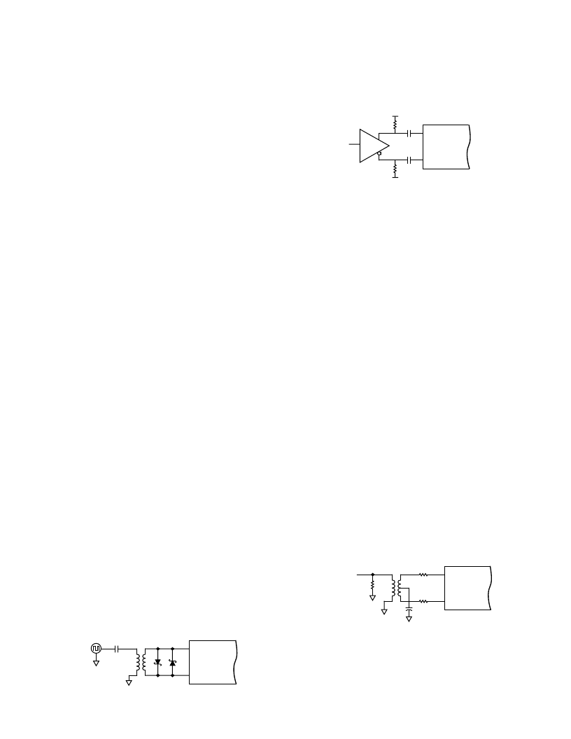
In applications where dc-coupling is required, a differential
output op amp such as the AD8138 from Analog Devices can
be used to drive the AD6645 (Figure 11). The AD8138 op amp
provides single-ended-to-differential conversion, which reduces
overall system cost and minimizes layout requirements.
相關PDF資料 |
PDF描述 |
|---|---|
| AD664BD-BIP | Monolithic 12-Bit Quad DAC |
| AD664BD-UNI | Monolithic 12-Bit Quad DAC |
| AD664JN-BIP | Monolithic 12-Bit Quad DAC |
| AD664JN-UNI | Monolithic 12-Bit Quad DAC |
| AD664JP | Monolithic 12-Bit Quad DAC |
相關代理商/技術參數(shù) |
參數(shù)描述 |
|---|---|
| AD6645ASQZ-105 | 制造商:Analog Devices 功能描述:ADC Single Pipelined 105Msps 14-bit Parallel 52-Pin LQFP EP 制造商:Analog Devices 功能描述:IC 14-BIT ADC |
| AD6645ASQZ-1051 | 制造商:AD 制造商全稱:Analog Devices 功能描述:14-Bit, 80 MSPS/105 MSPS A/D Converter |
| AD6645ASQZ-80 | 制造商:Analog Devices 功能描述:IC 14BIT ADC 80MSPS SMD LQFP52 |
| AD6645ASQZ-80 | 制造商:Analog Devices 功能描述:IC 14-BIT ADC |
| AD6645ASQZ-801 | 制造商:AD 制造商全稱:Analog Devices 功能描述:14-Bit, 80 MSPS/105 MSPS A/D Converter |
發(fā)布緊急采購,3分鐘左右您將得到回復。