- 您現(xiàn)在的位置:買賣IC網(wǎng) > PDF目錄373911 > AD7628 (Analog Devices, Inc.) ECONOLINE: REC2.2-S_DRW(Z)/H* - 2.2W DIP Package- 1kVDC Isolation- Regulated Output- 4.5-9V, 9-18V, 18-36V, 36-72V Wide Input Range 2 : 1- UL94V-0 Package Material- Continuous Short Circiut Protection- Cost Effective- 100% Burned In- Efficiency to 84% PDF資料下載
參數(shù)資料
| 型號: | AD7628 |
| 廠商: | Analog Devices, Inc. |
| 英文描述: | ECONOLINE: REC2.2-S_DRW(Z)/H* - 2.2W DIP Package- 1kVDC Isolation- Regulated Output- 4.5-9V, 9-18V, 18-36V, 36-72V Wide Input Range 2 : 1- UL94V-0 Package Material- Continuous Short Circiut Protection- Cost Effective- 100% Burned In- Efficiency to 84% |
| 中文描述: | CMOS雙8位緩沖乘法DAC |
| 文件頁數(shù): | 4/8頁 |
| 文件大小: | 193K |
| 代理商: | AD7628 |
AD7628
–4–
REV. A
INT E RFACE LOGIC INFORMAT ION
DAC Selection
Both DAC latches share a common 8-bit input port. T he con-
trol input
DAC A
/DAC B selects which DAC can accept data
from the input port.
Mode Selection
Inputs
CS
and
WR
control the operating mode of the selected
DAC. See Mode Selection T able below.
Write Mode
When
CS
and
WR
are both low, the selected DAC is in the write
mode. T he input data latches of the selected DAC are transpar-
ent and its analog output responds to activity on DB0–DB7.
Hold Mode
T he selected DAC latch retains the data that was present on
DB0–DB7 just prior to
CS
or
WR
assuming a high state. Both
analog outputs remain at the values corresponding to the data in
their respective latches.
Mode Selection T able
DAC A
/
DAC B
L
H
X
X
CS
WR
DAC A
WRIT E
HOLD
HOLD
HOLD
DAC B
HOLD
WRIT E
HOLD
HOLD
L
L
H
X
L
L
X
H
L = Low State, H = High State, X = Don’t Care
WRIT E CY CLE T IMING DIAGRAM
CIRCUIT INFORMAT ION—D/A SE CT ION
T he AD7628 contains two identical 8-bit multiplying D/A con-
verters, DAC A and DAC B. Each DAC consists of a highly
stable thin film R-2R ladder and eight N-channel current steering
switches. A simplified D/A circuit for DAC A is shown in Figure
1. An inverted R-2R ladder structure is used; that is, binary
Figure 1. Simplified Functional Circuit for DAC A
weighted currents are switched between the DAC output and
AGND, thus maintaining fixed currents in each ladder leg inde-
pendent of switch state.
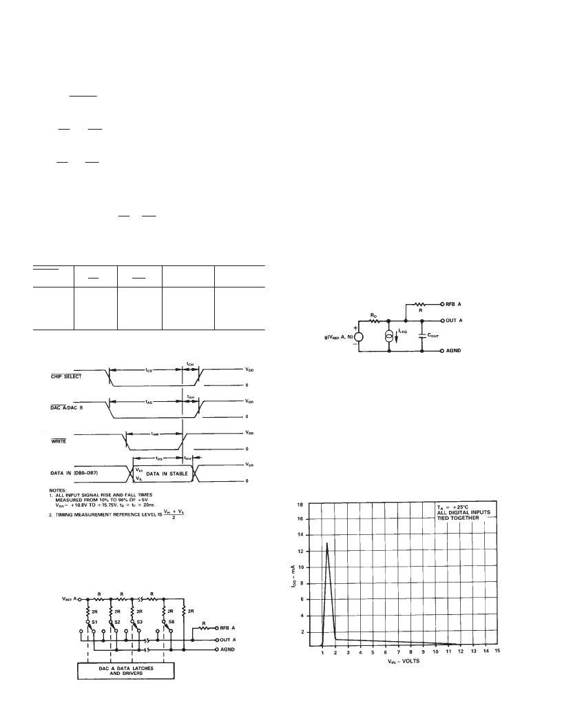
E QUIVALE NT CIRCUIT ANALY SIS
Figure 2 shows an approximate equivalent circuit for one of
the AD7628’s D/A converters, in this case DAC A. A similar
equivalent circuit can be drawn for DAC B. Note that AGND
(Pin 1) is common for both DAC A and DAC B.
T he current source I
LEAK AGE
is composed of surface and junc-
tion leakages and, as with most semiconductor devices, approxi-
mately doubles every 10
°
C. T he resistor Ro, as shown in Fig-
ure 2, is the equivalent output resistance of the device, which
varies with input code (excluding all 0s code) from 0.8R to 2R.
R is typically 11 k
. C
OUT
is the capacitance due to the N-channel
switches and varies from about 50 pF to 120 pF, depending on
the digital input. g(V
REF
A, N) is the T hevenin equivalent volt-
age generator due to the reference input voltage V
REF
A and the
transfer function of the R-2R ladder.
For further information on CMOS multiplying D/A converters,
refer to “CMOS DAC Application Guide, 2ND Edition” avail-
able from Analog Devices, Publication Number G872a–15–4/86.
Figure 2. Equivalent Analog Output Circuit of DAC A
CIRCUIT INFORMAT ION–DIGIT AL SE CT ION
T he input buffers are simple CMOS level-shifters designed so
that when the AD7628 is operated with V
DD
from 10.8 V to
15.75 V, the buffer converts T T L input levels (2.4 V and 0.8 V)
into CMOS logic levels. When V
IN
is in the region of 1.0 volt to
2.0 volts, the input buffers operate in their linear region and
pass a quiescent current (see Figure 3). T o minimize power sup-
ply currents, it is recommended that the digital input voltages be as
close to the supply rails (V
DD
and DGND) as practicably possible.
T he AD7628 may be operated with any supply voltage in the
range 10.8
≤
V
DD
≤
15.75 volts.
Figure 3. Typical Plot of Supply Current, I
DD
vs. Logic
Input Voltage V
IN
to V
DD
= +15 V
相關(guān)PDF資料 |
PDF描述 |
|---|---|
| AD7628BQ | CMOS Dual 8-Bit Buffered Multiplying DAC |
| AD7628KN | CMOS Dual 8-Bit Buffered Multiplying DAC |
| AD7628KP | ECONOLINE: REC2.2-S_DRW(Z)/H* - 2.2W DIP Package- 1kVDC Isolation- Regulated Output- 4.5-9V, 9-18V, 18-36V, 36-72V Wide Input Range 2 : 1- UL94V-0 Package Material- Continuous Short Circiut Protection- Cost Effective- 100% Burned In- Efficiency to 84% |
| AD7628KR | CMOS Dual 8-Bit Buffered Multiplying DAC |
| AD7628TE | CMOS Dual 8-Bit Buffered Multiplying DAC |
相關(guān)代理商/技術(shù)參數(shù) |
參數(shù)描述 |
|---|---|
| AD7628BFN | 制造商:未知廠家 制造商全稱:未知廠家 功能描述:8-Bit Digital-to-Analog Converter |
| AD7628BN | 制造商:未知廠家 制造商全稱:未知廠家 功能描述:8-Bit Digital-to-Analog Converter |
| AD7628BQ | 制造商:Rochester Electronics LLC 功能描述:- Bulk |
| AD7628KC/D | 制造商:未知廠家 制造商全稱:未知廠家 功能描述:8-Bit Digital-to-Analog Converter |
| AD7628KCWP | 制造商:未知廠家 制造商全稱:未知廠家 功能描述:8-Bit Digital-to-Analog Converter |
發(fā)布緊急采購,3分鐘左右您將得到回復。