- 您現(xiàn)在的位置:買賣IC網(wǎng) > PDF目錄373961 > AD9235BCP-20 (ANALOG DEVICES INC) 12-Bit, 20/40/65 MSPS 3 V A/D Converter PDF資料下載
參數(shù)資料
| 型號(hào): | AD9235BCP-20 |
| 廠商: | ANALOG DEVICES INC |
| 元件分類: | ADC |
| 英文描述: | 12-Bit, 20/40/65 MSPS 3 V A/D Converter |
| 中文描述: | 1-CH 12-BIT PROPRIETARY METHOD ADC, PARALLEL ACCESS, QCC32 |
| 封裝: | MO-220-VHHD-2, LFCSP-32 |
| 文件頁(yè)數(shù): | 14/32頁(yè) |
| 文件大小: | 1181K |
| 代理商: | AD9235BCP-20 |
第1頁(yè)第2頁(yè)第3頁(yè)第4頁(yè)第5頁(yè)第6頁(yè)第7頁(yè)第8頁(yè)第9頁(yè)第10頁(yè)第11頁(yè)第12頁(yè)第13頁(yè)當(dāng)前第14頁(yè)第15頁(yè)第16頁(yè)第17頁(yè)第18頁(yè)第19頁(yè)第20頁(yè)第21頁(yè)第22頁(yè)第23頁(yè)第24頁(yè)第25頁(yè)第26頁(yè)第27頁(yè)第28頁(yè)第29頁(yè)第30頁(yè)第31頁(yè)第32頁(yè)
REV. B
AD9235
–14–
The SHA may be driven from a source that keeps the signal
peaks within the allowable range for the selected reference volt-
age. The minimum and maximum common-mode input levels
are defined as follows:
VCM
VCM
The minimum common-mode input level allows the AD9235 to
accommodate ground-referenced inputs.
Although optimum performance is achieved with a differential
input, a single-ended source may be driven into VIN+ or VIN–.
In this configuration, one input will accept the signal, while the
opposite input should be set to midscale by connecting it to an
appropriate reference. For example, a 2 V p-p signal may be
applied to VIN+ while a 1 V reference is applied to VIN–. The
AD9235 will then accept an input signal varying between 2 V and
0 V. In the single-ended configuration, distortion performance may
degrade significantly as compared to the differential case. However,
the effect will be less noticeable at lower input frequencies and
in the lower speed grade models (AD9235-40 and AD9235-20).
Differential Input Configurations
As previously detailed, optimum performance will be achieved
while driving the AD9235 in a differential input configuration.
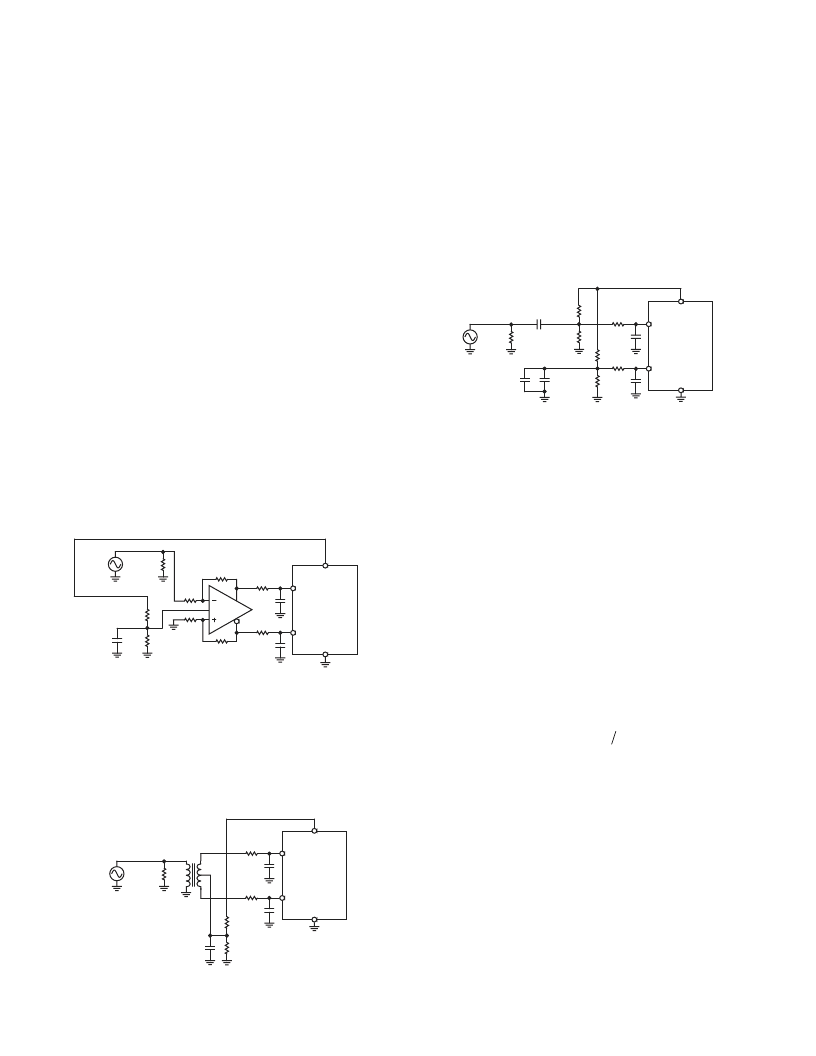
For baseband applications, the AD8138 differential driver provides
excellent performance and a flexible interface to the ADC. The
output common-mode voltage of the AD8138 is easily set to
AVDD/2, and the driver can be configured in a Sallen Key filter
topology to provide band limiting of the input signal.
VREF
MIN
=
/2
AVDD VREF
MAX
=
(
)/2
AD9235
VIN+
VIN–
AVDD
1Vp-p
49.9
523
1k
1k
0.1 F
22
22
15pF
15pF
499
499
499
AD8138
AGND
Figure 8. Differential Input Configuration Using
the AD8138
At input frequencies in the second Nyquist zone and above, the
performance of most amplifiers will not be adequate to achieve
the true performance of the AD9235. This is especially true in
IF undersampling applications where frequencies in the 70 MHz
to 100 MHz range are being sampled. For these applications,
differential transformer coupling is the recommended input
configuration, as shown in Figure 9.
AD9235
VIN+
VIN–
AVDD
AGND
22
22
15pF
15pF
49.9
1k
1k
0.1 F
2V p-p
Figure 9. Differential Transformer-Coupled Configuration
The signal characteristics must be considered when selecting a
transformer. Most RF transformers will saturate at frequencies
below a few MHz, and excessive signal power can also cause core
saturation, which leads to distortion.
Single-Ended Input Configuration
A single-ended input may provide adequate performance in
cost-sensitive applications. In this configuration, there will be a
degradation in SFDR and in distortion performance due to the
large input common-mode swing. However, if the source
impedances on each input are matched, there should be little effect
on SNR performance. Figure 10 details a typical single-ended
input configuration.
AD9235
VIN+
VIN–
AVDD
AGND
2Vp-p
22
22
15pF
15pF
49.9
1k
1k
0.33 F
10 F
0.1 F
1k
1k
+
Figure 10. Single-Ended Input Configuration
CLOCK INPUT CONSIDERATIONS
Typical high speed ADCs use both clock edges to generate a
variety of internal timing signals, and as a result may be sensitive to
clock duty cycle. Commonly a 5% tolerance is required on the
clock duty cycle to maintain dynamic performance character-
istics. The AD9235 contains a clock duty cycle stabilizer (DCS)
that retimes the nonsampling edge, providing an internal clock
signal with a nominal 50% duty cycle. This allows a wide range
of clock input duty cycles without affecting the performance of the
AD9235. As shown in TPC 20, noise and distortion perfor-
mance are nearly flat over a 30% range of duty cycle.
The duty cycle stabilizer uses a delay-locked loop (DLL) to
create the nonsampling edge. As a result, any changes to the
sampling frequency will require approximately 100 clock cycles
to allow the DLL to acquire and lock to the new rate.
High speed, high resolution ADCs are sensitive to the quality of
the clock input. The degradation in SNR at a given full-scale
input frequency (
f
INPUT
) due only to aperture jitter (
t
J
) can be
calculated with the following equation.
SNR Degradation
In the equation, the rms aperture jitter,
t
J
, represents the root-
sum square of all jitter sources, which include the clock input,
analog input signal, and ADC aperture jitter specification. Under-
sampling applications are particularly sensitive to jitter.
The clock input should be treated as an analog signal in cases
where aperture jitter may affect the dynamic range of the AD9235.
Power supplies for clock drivers should be separated from the
ADC output driver supplies to avoid modulating the clock signal
with digital noise. Low jitter, crystal-controlled oscillators make
the best clock sources. If the clock is generated from another
type of source (by gating, dividing, or other methods), it should
be retimed by the original clock at the last step.
f
t
INPUT
=
×
×
×
×
]
20
10 1 2
log
π
J
相關(guān)PDF資料 |
PDF描述 |
|---|---|
| AD9235BCP-40 | 12-Bit, 20/40/65 MSPS 3 V A/D Converter |
| AD9235BCP-65 | 12-Bit, 20/40/65 MSPS 3 V A/D Converter |
| AD9235BRU-20 | 12-Bit, 20/40/65 MSPS 3 V A/D Converter |
| AD9235BRU-40 | 12-Bit, 20/40/65 MSPS 3 V A/D Converter |
| AD9235BRU-65 | 12-Bit, 20/40/65 MSPS 3 V A/D Converter |
相關(guān)代理商/技術(shù)參數(shù) |
參數(shù)描述 |
|---|---|
| AD9235BCP-20EB | 制造商:Analog Devices 功能描述:EVAL BD FOR 12-BIT, 20/40/65 MSPS ,3V A/D CNVRTR - Bulk |
| AD9235BCP-20EBZ | 制造商:Analog Devices 功能描述:Evaluation Board For 12-Bit, 20/40/65 MSPS ,3 V A/D Converter 制造商:Analog Devices 功能描述:EVAL BD FOR 12-BIT, 20/40/65 MSPS ,3V A/D CNVRTR - Bulk |
| ad9235bcp-40 | 制造商:Analog Devices 功能描述:ADC SGL PIPELINED 40MSPS 12-BIT PARALLEL 32LFCSP EP - Bulk 制造商:Rochester Electronics LLC 功能描述: |
| AD9235BCP-40EB | 制造商:Analog Devices 功能描述:EVAL BD FOR 12-BIT, 20/40/65 MSPS ,3V A/D CNVRTR - Bulk |
| AD9235BCP-40EBZ | 制造商:Analog Devices 功能描述:Evaluation Board For 12-Bit, 20/40/65 MSPS ,3 V A/D Converter 制造商:Analog Devices 功能描述:EVAL BD FOR 12-BIT, 20/40/65 MSPS ,3V A/D CNVRTR - Bulk |
發(fā)布緊急采購(gòu),3分鐘左右您將得到回復(fù)。