- 您現(xiàn)在的位置:買賣IC網(wǎng) > PDF目錄373965 > AD9698KN (ANALOG DEVICES INC) Ultrafast TTL Comparators PDF資料下載
參數(shù)資料
| 型號: | AD9698KN |
| 廠商: | ANALOG DEVICES INC |
| 元件分類: | 運動控制電子 |
| 英文描述: | Ultrafast TTL Comparators |
| 中文描述: | DUAL COMPARATOR, 3000 uV OFFSET-MAX, PDIP16 |
| 封裝: | PLASTIC, DIP-16 |
| 文件頁數(shù): | 7/8頁 |
| 文件大小: | 135K |
| 代理商: | AD9698KN |
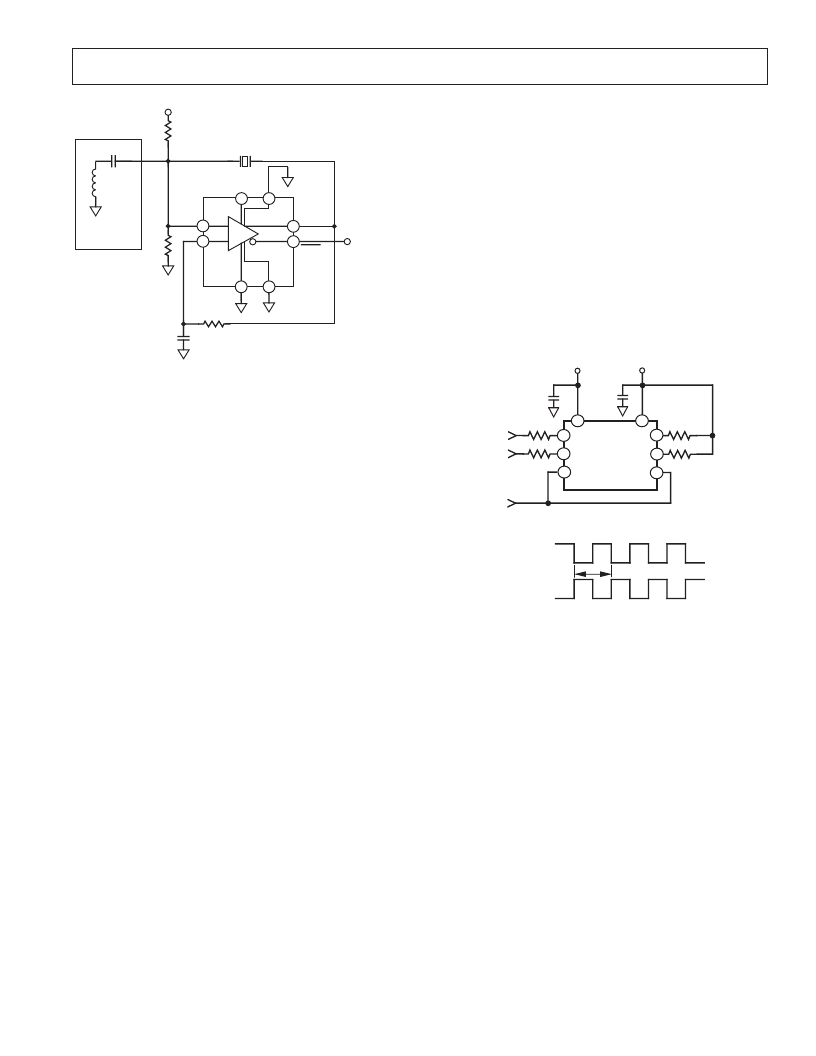
AD9696/AD9698
–7–
REV. B
2
AD9696
–IN
+IN
+V
S
1– 40MHz
LATCH
ENABLE
+
–
OSCILLATOR
OUTPUT
GROUND
Q
OUT
2k
+V
S
0.1μF
(220pF for Freq. > 10MHz)
0.1μF
FOR USE WITH
OVERTONE
CRYSTAL
(VALUE
DEPENDS
ON FREQ.)
3
1
5
7
8
4
6
2k
2k
Q
OUT
–V
S
Figure 2. AD9696 Oscillator Circuit (Based on DIP Pinouts)
When generating frequencies using a nonfundamental mode
crystal, a choke and dc blocking capacitor are added. As an ex-
ample, a 36 MHz oscillator can be achieved by using a 12 MHz
crystal operating on its third overtone. T o suppress oscillation at
the 12 MHz fundamental, the value of the choke is chosen to
provide a low reactive impedance at the fundamental frequency
while maintaining a high reactive impedance at the desired out-
put frequency (for 36 MHz operation, L = 1.8
μ
H). T he shunt
capacitor at the inverting input has a value of 220 pF for a stable
36 MHz frequency.
LAY OUT CONSIDE RAT IONS
When working with high speed circuits, proper layout is critical.
Analog signal paths should be kept as short as possible and be
properly terminated to avoid reflections. In addition, digital sig-
nal paths should be kept short, and run lengths should be mat-
ched to avoid propagation delay mismatch. All analog signals
should be kept as far away from digital signal paths as possible;
this reduces the amount of digital switching noise that might be
capacitively coupled into the analog section of the circuit.
In high speed circuits, layout of the ground circuit is the most
important factor. A single, low impedance ground plane, on the
component side of the board, will reduce noise in the circuit
ground. It is especially important to maintain continuity of the
ground plane under and around the AD9696 or AD9698.
Sockets limit the dynamic performance of the device and should
be used only for prototypes or evaluation.
8
7
6
5
4
3
2
1
AD9696
(8-PIN DIP)
0.1μF
0.1μF
AD1
AD2
GND
RESISTORS ARE 1k
±5%
– V
S
+V
S
5μs
–0.9V
AD1
AD2
–0.9 V
–1.7V
–1.7V
Burn-In Circuit
相關(guān)PDF資料 |
PDF描述 |
|---|---|
| AD9698KQ | Ultrafast TTL Comparators |
| AD9698KR | Ultrafast TTL Comparators |
| AD9698TQ | Ultrafast TTL Comparators |
| AD9696 | Ultrafast TTL Comparators |
| AD9696KN | Ultrafast TTL Comparators |
相關(guān)代理商/技術(shù)參數(shù) |
參數(shù)描述 |
|---|---|
| AD9698KQ | 制造商:AD 制造商全稱:Analog Devices 功能描述:Ultrafast TTL Comparators |
| AD9698KR | 制造商:AD 制造商全稱:Analog Devices 功能描述:Ultrafast TTL Comparators |
| AD9698TQ | 制造商:AD 制造商全稱:Analog Devices 功能描述:Ultrafast TTL Comparators |
| AD9698TQ/883B | 制造商:未知廠家 制造商全稱:未知廠家 功能描述:Analog Comparator |
| AD9698TZ/883B | 制造商:AD 制造商全稱:Analog Devices 功能描述:Ultrafast TTL Comparators |
發(fā)布緊急采購,3分鐘左右您將得到回復(fù)。