- 您現(xiàn)在的位置:買賣IC網(wǎng) > PDF目錄378281 > ADC10080CIMT (NATIONAL SEMICONDUCTOR CORP) 10-Bit, 80 MSPS, 3V, 78.6 mW A/D Converter PDF資料下載
參數(shù)資料
| 型號: | ADC10080CIMT |
| 廠商: | NATIONAL SEMICONDUCTOR CORP |
| 元件分類: | ADC |
| 英文描述: | 10-Bit, 80 MSPS, 3V, 78.6 mW A/D Converter |
| 中文描述: | 1-CH 10-BIT PROPRIETARY METHOD ADC, PARALLEL ACCESS, PDSO28 |
| 封裝: | TSSOP-28 |
| 文件頁數(shù): | 8/19頁 |
| 文件大小: | 927K |
| 代理商: | ADC10080CIMT |
Specification Definitions
APERTURE DELAY
is the time after the rising edge of the
clock to when the input signal is acquired or held for conver-
sion.
APERTURE JITTER (APERTURE UNCERTAINTY)
is the
variation in aperture delay from sample to sample. Aperture
jitter manifests itself as noise in the output.
COMMON MODE VOLTAGE (V
CM
)
is the d.c. potential
present at both signal inputs to the ADC.
CONVERSION LATENCY
See PIPELINE DELAY.
DIFFERENTIAL NON-LINEARITY (DNL)
is the measure of
the maximum deviation from the ideal step size of 1 LSB.
DUTY CYCLE
is the ratio of the time that a repetitive digital
waveform is high to the total time of one period. The speci-
fication here refers to the ADC clock input signal.
EFFECTIVE NUMBER OF BITS (ENOB, or EFFECTIVE
BITS)
is another method of specifying Signal-to-Noise and
Distortion or SINAD. ENOB is defined as (SINAD - 1.76) /
6.02 and states that the converter is equivalent to a perfect
ADC of this (ENOB) number of bits.
FULL POWER BANDWIDTH
is a measure of the frequency
at which the reconstructed output fundamental drops 3 dB
below its low frequency value for a full scale input.
GAIN ERROR
is the deviation from the ideal slope of the
transfer function. It can be calculated as:
Gain Error = Positive Full-Scale Error Negative Full-
Scale Error
INTEGRAL NON LINEARITY (INL)
is a measure of the
deviation of each individual code from a line drawn from
negative full scale (
1
2
LSB below the first code transition)
through positive full scale (
1
2
LSB above the last code
transition). The deviation of any given code from this straight
line is measured from the center of that code value.
MISSING CODES
are those output codes that will never
appear at the ADC outputs. The ADC10080 is guaranteed
not to have any missing codes.
NEGATIVE FULL SCALE ERROR
is the difference between
the input voltage (V
IN
+
V
IN
) just causing a transition from
negative full scale to the first code and its ideal value of
0.5 LSB.
OFFSET ERROR
is the input voltage that will cause a tran-
sition from a code of 01 1111 1111 to a code of 10 0000 0000.
OUTPUT DELAY
is the time delay after the rising edge of
the clock before the data update is presented at the output
pins.
PIPELINE DELAY (LATENCY)
is the number of clock cycles
between initiation of conversion and when that data is pre-
sented to the output driver stage. Data for any given sample
is available at the output pins the Pipeline Delay plus the
Output Delay after the sample is taken. New data is available
at every clock cycle, but the data lags the conversion by the
pipeline delay.
POSITIVE FULL SCALE ERROR
is the difference between
the actual last code transition and its ideal value of 1
1
2
LSB
below positive full scale.
SIGNAL TO NOISE RATIO (SNR)
is the ratio, expressed in
dB, of the rms value of the input signal to the rms value of the
sum of all other spectral components below one-half the
sampling frequency, not including harmonics or dc.
SIGNAL TO NOISE PLUS DISTORTION (S/N+D or SINAD)
Is the ratio, expressed in dB, of the rms value of the input
signal to the rms value of all of the other spectral compo-
nents below half the clock frequency, including harmonics
but excluding dc.
SPURIOUS FREE DYNAMIC RANGE (SFDR)
is the differ-
ence, expressed in dB, between the rms values of the input
signal and the peak spurious signal, where a spurious signal
is any signal present in the output spectrum that is not
present at the input.
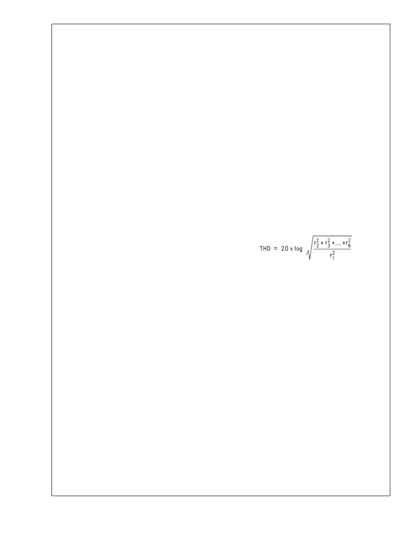
TOTAL HARMONIC DISTORTION (THD)
is the ratio, ex-
pressed in dBc, of the rms total of the first six harmonic
levels at the output to the level of the fundamental at the
output. THD is calculated as:
where f
is the RMS power of the fundamental (output)
frequency and f
through f
6
are the RMS power in the first 6
harmonic frequencies.
Second Harmonic Distortion (2nd Harm)
is the difference
expressed in dB, between the RMS power in the input
frequency at the output and the power in its 2nd harmonic
level at the output.
Third Harmonic Distortion (3rd Harm)
is the difference,
expressed in dB, between the RMS power in the input
frequency at the output and the power in its 3rd harmonic
level at the output.
A
www.national.com
8
相關(guān)PDF資料 |
PDF描述 |
|---|---|
| ADC10080 | 10-Bit, 80 MSPS, 3V, 78.6 mW A/D Converter |
| ADC10154CIWM | 10-Bit Plus Sign 4 レs ADCs with 4- or 8-Channel MUX, Track/Hold and Reference |
| ADC10158CIWM | 10-Bit Plus Sign 4 レs ADCs with 4- or 8-Channel MUX, Track/Hold and Reference |
| ADC10154 | Low-Voltage High-Speed Quadruple Differential Line Receiver 16-SOIC 0 to 70 |
| ADC10158 | Low-Voltage High-Speed Quadruple Differential Line Receiver 16-SOIC 0 to 70 |
相關(guān)代理商/技術(shù)參數(shù) |
參數(shù)描述 |
|---|---|
| ADC10080CIMT | 制造商:Texas Instruments 功能描述:IC 10BIT ADC 80MSPS 3V POWERWISE |
| ADC10080CIMT/NOPB | 功能描述:模數(shù)轉(zhuǎn)換器 - ADC RoHS:否 制造商:Texas Instruments 通道數(shù)量:2 結(jié)構(gòu):Sigma-Delta 轉(zhuǎn)換速率:125 SPs to 8 KSPs 分辨率:24 bit 輸入類型:Differential 信噪比:107 dB 接口類型:SPI 工作電源電壓:1.7 V to 3.6 V, 2.7 V to 5.25 V 最大工作溫度:+ 85 C 安裝風格:SMD/SMT 封裝 / 箱體:VQFN-32 |
| ADC10080CIMTX | 功能描述:模數(shù)轉(zhuǎn)換器 - ADC RoHS:否 制造商:Texas Instruments 通道數(shù)量:2 結(jié)構(gòu):Sigma-Delta 轉(zhuǎn)換速率:125 SPs to 8 KSPs 分辨率:24 bit 輸入類型:Differential 信噪比:107 dB 接口類型:SPI 工作電源電壓:1.7 V to 3.6 V, 2.7 V to 5.25 V 最大工作溫度:+ 85 C 安裝風格:SMD/SMT 封裝 / 箱體:VQFN-32 |
| ADC10080CIMTX/NOPB | 功能描述:模數(shù)轉(zhuǎn)換器 - ADC RoHS:否 制造商:Texas Instruments 通道數(shù)量:2 結(jié)構(gòu):Sigma-Delta 轉(zhuǎn)換速率:125 SPs to 8 KSPs 分辨率:24 bit 輸入類型:Differential 信噪比:107 dB 接口類型:SPI 工作電源電壓:1.7 V to 3.6 V, 2.7 V to 5.25 V 最大工作溫度:+ 85 C 安裝風格:SMD/SMT 封裝 / 箱體:VQFN-32 |
| ADC10080EVAL | 功能描述:數(shù)據(jù)轉(zhuǎn)換 IC 開發(fā)工具 ADC10080 EVAL BOARD RoHS:否 制造商:Texas Instruments 產(chǎn)品:Demonstration Kits 類型:ADC 工具用于評估:ADS130E08 接口類型:SPI 工作電源電壓:- 6 V to + 6 V |
發(fā)布緊急采購,3分鐘左右您將得到回復。