- 您現(xiàn)在的位置:買賣IC網(wǎng) > PDF目錄378281 > ADC10080CIMTX (NATIONAL SEMICONDUCTOR CORP) 10-Bit, 80 MSPS, 3V, 78.6 mW A/D Converter PDF資料下載
參數(shù)資料
| 型號(hào): | ADC10080CIMTX |
| 廠商: | NATIONAL SEMICONDUCTOR CORP |
| 元件分類: | ADC |
| 英文描述: | 10-Bit, 80 MSPS, 3V, 78.6 mW A/D Converter |
| 中文描述: | 1-CH 10-BIT PROPRIETARY METHOD ADC, PARALLEL ACCESS, PDSO28 |
| 封裝: | TSSOP-28 |
| 文件頁(yè)數(shù): | 16/19頁(yè) |
| 文件大?。?/td> | 927K |
| 代理商: | ADC10080CIMTX |
第1頁(yè)第2頁(yè)第3頁(yè)第4頁(yè)第5頁(yè)第6頁(yè)第7頁(yè)第8頁(yè)第9頁(yè)第10頁(yè)第11頁(yè)第12頁(yè)第13頁(yè)第14頁(yè)第15頁(yè)當(dāng)前第16頁(yè)第17頁(yè)第18頁(yè)第19頁(yè)
Functional Description
The ADC10080 uses a pipeline architecture and has error
correction circuitry to help ensure maximum performance.
Differential analog input signals are digitized to 10 bits. In
differential mode each analog input signal should have a
peak-to-peak voltage equal to 1.0V, 0.75V or 0.5V, depend-
ing on the state of the IRS pin (pin 5), and be centered
around V
CM
and be 180 out of phase with each other. If
single ended operation is desired, V
IN
- may be tied to the
V
COM
pin (pin 4). A single ended input signal may then be
applied to V
IN
+, and should have an average value in the
range of V
CM
. The signal amplitude should be 2.0V, 1.5V or
1.0V peak-to-peak, depending on the state or the IRS pin
(pin 5).
Applications Information
1.0 ANALOG INPUTS
TheADC10080 has two analog signal inputs, V
+ and V
.
These two pins form a differential input pair. There is one
common mode pin V
that may be used to set the com-
mon mode input voltage.
1.1 REFERENCE PINS
TheADC10080 is designed to operate with a 1.2V reference,
but performs well with reference voltages in the range of
0.8V to 2.0V. Lower reference voltages will decrease the
signal-to-noise ratio (SNR) of the ADC10080. It is very im-
portant that all grounds associated with the reference volt-
age and the input signal make connection to the analog
ground plane at a single point to minimize the effects of
noise currents in the ground path. The three Reference
Bypass Pins V
REF
, V
REFT
and V
REFB
, are made available for
bypass purposes only. These pins should each be bypassed
to ground with a 0.1 μF capacitor. DO NOT LOAD these pins.
1.2 V
COM
PIN
This pin supplies a voltage for possible use to set the com-
mon mode input voltage. This pin may also be connected to
V
IN
-, so that V
IN
+ may be used as a single ended input. This
pin should be byassed with at least a 0.1 uF capacitor.
1.3 SIGNAL INPUTS
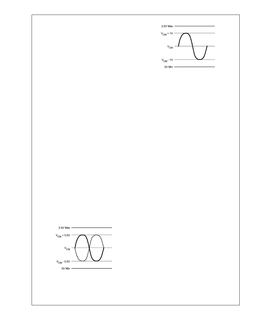
The signal inputs are V
+ and V
. The input signal ampli-
tude is defined as V
IN
+ V
IN
and is represented schemati-
cally in
Figure 3:
A single ended input signal is shown in
Figure 4.
The internal switching action at the analog inputs causes
energy to be output from the input pins.As the driving source
tries to compensate for this, it adds noise to the signal. To
prevent this, use 18
series resistors at each of the signal
inputs with a 25 pF capacitor across the inputs, as can be
seen in
Figure 5
. These components should be placed close
to the ADC because the input pins of the ADC is the most
sensitive part of the system and this is the last opportunity to
filter the input. The two 18
resistors and the 25 pF capaci-
tor form a low-pass filter with a -3 dB frequency of 177 MHz
.
1.4 CLK PIN
The CLK signal controls the timing of the sampling process.
Drive the clock input with a stable, low jitter clock signal in
the range of 20 MHz to 80 MHz with rise and fall times of less
than 2 ns. The trace carrying the clock signal should be as
short as possible and should not cross any other signal line,
analog or digital, not even at 90. The CLK signal also drives
an internal state machine. If the CLK is interrupted, or its
frequency is too low, the charge on internal capacitors can
dissipate to the point where the accuracy of the output data
will degrade. This is what limits the lowest sample rate to
20 MSPS. The duty cycle of the clock signal can affect the
performance of any A/D Converter. Because achieving a
precise duty cycle is difficult, the ADC10080 is designed to
maintain performance over a range of duty cycles. While it is
specified and performance is guaranteed with a 50% clock
duty cycle, performance is typically maintained over a clock
duty cycle range of 40% to 60%.
1.5 STBY PIN
The STBY pin, when high, holds the ADC10080 in a power-
down mode to conserve power when the converter is not
being used. The power consumption in this state is 15 mW.
The output data pins are undefined in this mode. Power
consumption during power-down is not affected by the clock
frequency, or by whether there is a clock signal present. The
data in the pipeline is corrupted while in the power down.
1.6 DF PIN
The DF pin, when high, forces the ADC10080 to output the
2’s complement data format. When DF is tied low, the output
format is offset binary.
1.7 IRS PIN
The IRS (Input Range Select) pin defines the input signal
amplitude that will produce a full scale output. The table
below describes the function of the IRS pin.
20048547
FIGURE 3. Input Voltage Waveforms for a 2V
P-P
Differential Input
20048548
FIGURE 4. Input Voltage Waveform for a 2V
P-P
Single
Ended Input
A
www.national.com
16
相關(guān)PDF資料 |
PDF描述 |
|---|---|
| ADC10080CIMT | 10-Bit, 80 MSPS, 3V, 78.6 mW A/D Converter |
| ADC10080 | 10-Bit, 80 MSPS, 3V, 78.6 mW A/D Converter |
| ADC10154CIWM | 10-Bit Plus Sign 4 レs ADCs with 4- or 8-Channel MUX, Track/Hold and Reference |
| ADC10158CIWM | 10-Bit Plus Sign 4 レs ADCs with 4- or 8-Channel MUX, Track/Hold and Reference |
| ADC10154 | Low-Voltage High-Speed Quadruple Differential Line Receiver 16-SOIC 0 to 70 |
相關(guān)代理商/技術(shù)參數(shù) |
參數(shù)描述 |
|---|---|
| ADC10080CIMTX/NOPB | 功能描述:模數(shù)轉(zhuǎn)換器 - ADC RoHS:否 制造商:Texas Instruments 通道數(shù)量:2 結(jié)構(gòu):Sigma-Delta 轉(zhuǎn)換速率:125 SPs to 8 KSPs 分辨率:24 bit 輸入類型:Differential 信噪比:107 dB 接口類型:SPI 工作電源電壓:1.7 V to 3.6 V, 2.7 V to 5.25 V 最大工作溫度:+ 85 C 安裝風(fēng)格:SMD/SMT 封裝 / 箱體:VQFN-32 |
| ADC10080EVAL | 功能描述:數(shù)據(jù)轉(zhuǎn)換 IC 開發(fā)工具 ADC10080 EVAL BOARD RoHS:否 制造商:Texas Instruments 產(chǎn)品:Demonstration Kits 類型:ADC 工具用于評(píng)估:ADS130E08 接口類型:SPI 工作電源電壓:- 6 V to + 6 V |
| ADC100C | 制造商:未知廠家 制造商全稱:未知廠家 功能描述:Precision 22 Bit Integrating A/D Converter |
| ADC100CA | 制造商:未知廠家 制造商全稱:未知廠家 功能描述:Precision 22 Bit Integrating A/D Converter |
| ADC100M | 制造商:未知廠家 制造商全稱:未知廠家 功能描述:Precision 22 Bit Integrating A/D Converter |
發(fā)布緊急采購(gòu),3分鐘左右您將得到回復(fù)。