- 您現在的位置:買賣IC網 > PDF目錄378281 > ADC10462CIWMX (NATIONAL SEMICONDUCTOR CORP) 10-Bit 600 ns A/D Converter with Input Multiplexer and Sample/Hold PDF資料下載
參數資料
| 型號: | ADC10462CIWMX |
| 廠商: | NATIONAL SEMICONDUCTOR CORP |
| 元件分類: | ADC |
| 英文描述: | 10-Bit 600 ns A/D Converter with Input Multiplexer and Sample/Hold |
| 中文描述: | 2-CH 10-BIT FLASH METHOD ADC, PARALLEL ACCESS, PDSO24 |
| 封裝: | SOP-24 |
| 文件頁數: | 12/15頁 |
| 文件大小: | 342K |
| 代理商: | ADC10462CIWMX |
Applications Information
(Continued)
4.0 INHERENT SAMPLE-AND-HOLD
Because
the ADC10461, ADC10462,
sample the input signal once during each conversion, they
are capable of measuring relatively fast input signals without
the help of an external sample-hold. In a non-sampling
successive-approximation A/D converter, regardless of
speed, the input signal must be stable to better than
±
1/2
LSB during each conversion cycle or significant errors will
result. Consequently, even for many relatively slow input
signals, the signals must be externally sampled and held
constant during each conversion if a SAR with no internal
sample-and-hold is used.
Because they incorporate a direct sample/hold control input,
the ADC10461, ADC10462, and ADC10464 are suitable for
use in DSP-based systems. The S /H input allows synchro-
nization of the A/D converter to the DSP system’s sampling
rate
and
to
other
ADC10461s,
ADC10464s.
The ADC10461, ADC10462, and ADC10464 can perform
accurate conversions of input signals with frequency compo-
nents from DC to over 250 kHz.
and ADC10464
ADC10462s,
and
5.0 POWER SUPPLY CONSIDERATIONS
The ADC10461, ADC10462, and ADC10464 are designed to
operate from a +5V (nominal) power supply. There are two
supply pins, AV
and DV
. These pins allow separate
external bypass capacitors for the analog and digital portions
of the circuit. To guarantee accurate conversions, the two
supply pins should be connected to the same voltage
source, and each should be bypassed with a 0.1 μF ceramic
capacitor in parallel with a 10 μF tantalum capacitor. De-
pending on the circuit board layout and other system con-
siderations, more bypassing may be necessary.
The ADC10461 has a single ground pin, and the ADC10462
and ADC10464 each have separate analog and digital
ground pins for separate bypassing of the analog and digital
supplies. The devices with separate analog and digital
ground pins should have their ground pins connected to the
same potential, and all grounds should be “clean” and free of
noise.
In systems with multiple power supplies, careful attention to
power supply sequencing may be necessary to avoid over-
driving inputs. The A/D converter’s power supply pins should
be at the proper voltage before digital or analog signals are
applied to any of the other pins.
6.0 LAYOUT AND GROUNDING
In order to ensure fast, accurate conversions from the
ADC10461, ADC10462, and ADC10464, it is necessary to
use appropriate circuit board layout techniques. The analog
ground return path should be low-impedance and free of
noise from other parts of the system. Noise from digital
circuitry can be especially troublesome, so digital grounds
should always be separate from analog grounds. For best
performance, separate ground planes should be provided for
the digital and analog parts of the system.
All bypass capacitors should be located as close to the
converter as possible and should connect to the converter
and to ground with short traces. The analog input should be
isolated from noisy signal traces to avoid having spurious
signals couple to the input. Any external component (e.g., a
filter capacitor) connected across the converter’s input
should be connected to a very clean ground return point.
Grounding the component at the wrong point will result in
reduced conversion accuracy.
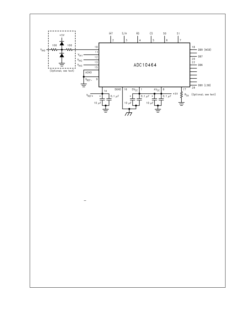
01110814
FIGURE 4. Typical Connection. Note the multiple bypass capacitors on the reference and power supply pins. If V
REF
is not grounded, it should also be bypassed to analog ground using multiple capacitors (see 5.0 “Power Supply
Considerations”). AGND and DGND should be at the same potential. V
is shown with an input protection network.
Pin 17 is normally left open, but optional “speedup” resistor R
SA
can be used to reduce the conversion time.
A
www.national.com
12
相關PDF資料 |
PDF描述 |
|---|---|
| ADC10464CIWMX | 10-Bit 600 ns A/D Converter with Input Multiplexer and Sample/Hold |
| ADC10462 | 10-Bit 600 ns A/D Converter with Input Multiplexer and Sample/Hold(10位 600 ns帶輸入多路器和采樣/保持功能的A/D轉換器) |
| ADC10464 | 10-Bit 600 ns A/D Converter with Input Multiplexer and Sample/Hold(10位 600 ns帶輸入多路器和采樣/保持功能的A/D轉換器) |
| ADC104S051 | Switch-mode Multi-Chemistry Battery Charger with Peak Voltage Detection Termination 8-PDIP -20 to 70 |
| ADC104S101 | 4 Channel, 1 MSPS, 10-Bit A/D Converter |
相關代理商/技術參數 |
參數描述 |
|---|---|
| ADC10462CIWMX/NOPB | 制造商:Texas Instruments 功能描述:ADC Single 800ksps 10-bit Parallel 24-Pin SOIC W T/R |
| ADC10462CMJ | 制造商:未知廠家 制造商全稱:未知廠家 功能描述:Single-Ended Data Acquisition System |
| ADC10464 | 制造商:NSC 制造商全稱:National Semiconductor 功能描述:10-Bit 600 ns A/D Converter with Input Multiplexer and Sample/Hold |
| ADC10464CIJ | 制造商:未知廠家 制造商全稱:未知廠家 功能描述:Single-Ended Data Acquisition System |
| ADC10464CIWM | 功能描述:模數轉換器 - ADC RoHS:否 制造商:Texas Instruments 通道數量:2 結構:Sigma-Delta 轉換速率:125 SPs to 8 KSPs 分辨率:24 bit 輸入類型:Differential 信噪比:107 dB 接口類型:SPI 工作電源電壓:1.7 V to 3.6 V, 2.7 V to 5.25 V 最大工作溫度:+ 85 C 安裝風格:SMD/SMT 封裝 / 箱體:VQFN-32 |
發(fā)布緊急采購,3分鐘左右您將得到回復。